Dissertation
zur Erlangung des Doktorgrades der Naturwissenschaften (Dr. rer. nat.) der Fakultät für Physik der Universität
Regensburg
Thermal Transport across
Atomic and Molecular Junctions
vorgelegt von Nico Mosso
2018
Promotionsgesuch eingereicht am 28. Mai 2018.
Die Arbeit wurde angeleitet von
Dr. Bernd Gotsmann und Prof. Dr. Jascha Repp.
Prüfungsausschuss
Vorsitzender: Prof. Dr. Tilo Wettig 1. Gutachter: Prof. Dr. Jascha Repp 2. Gutachter: Prof. Dr. Christoph Strunk Weiterer Prüfer: PD. Dr. Andreas Hüttel
Termin Promotionskolloquium: 26. Oktober 2018
When you can measure what you are speaking about. . . you know something about it.
- Lord Kelvin, 1883
Table of Contents
1. Introduction 3
1.1 Outline . . . 4
2. Background 6 2.1 Charge Transport . . . 6
2.1.1 Conductance Quantization in Metallic Quantum Point Contacts 9 2.1.2 Molecular Junctions . . . 11
2.1.3 Electronic thermal transport and thermoelectric effects . . . 14
2.2 Phonon Transport . . . 15
3. Experimental Setup 18 3.1 Experimental Setup . . . 18
3.1.1 Introduction . . . 18
3.1.2 Working principle . . . 19
3.1.3 The setup . . . 20
3.1.4 Noise Free Labs . . . 22
3.1.5 Data acquisition and system control . . . 24
3.1.6 The electrical circuits . . . 25
3.2 MEMS design, fabrication and characterization . . . 29
3.2.1 Noise performance . . . 30
3.2.2 Fabrication Process . . . 31
3.2.3 MEMS design . . . 32
3.2.4 MEMS characterization . . . 36
3.3 Sample preparation . . . 41
3.3.1 Cleanliness of the gold platform on the MEMS . . . 42
3.3.2 Gold surface functionalization . . . 44
3.3.3 STM tip preparation . . . 45
4. Metallic Quantum Point Contacts 48 4.1 Gold-gold contacts . . . 48
4.1.1 Phonon contribution to the thermal conductance . . . 54
4.1.2 Heat transport properties of gold contacts with small organic molecules . . . 56
4.1.3 Power dissipation in atomic contacts . . . 58
4.1.4 Thermal background . . . 58
4.1.5 Uncertainty calculation . . . 60
4.1.6 Angled approach . . . 61
4.1.7 Gold surface roughness . . . 62
4.1.8 Tip temperature . . . 63
4.1.9 Data analysis procedure . . . 64
4.2 Pt-Pt contacts . . . 64
4.3 Metallic hetero-junctions . . . 66
5. Single Molecule Junctions 69 5.1 Introduction . . . 69
5.2 Experimental results . . . 70
5.2.1 Experimental results with octane-dithiol molecular junctions 75 5.2.2 Reproducibility of the measurements . . . 77
5.3 Sample preparation . . . 83
5.4 Uncertainty calculation of experimental data . . . 84
5.5 Comparison with theory and previous experiments . . . 85
6. Conclusions and Outlook 91 6.1 Outlook . . . 92
A. Power dissipation and temperature distribution along the supporting beams 94 B. Tip etching with different metals 96 B.1 Pt and Pt-Ir tips . . . 96
B.2 W tips . . . 97
Chapter 1
Introduction
Heat dissipation has been widely recognized as one of the main limiting factors of the performances of nanoscale electronics devices [1, 2]. Apart from these challenges, engineering the thermal transport properties of materials is highly desirable for thermoelectric, cooling [3] and more in general thermal management applications.
Heat transport in molecular junctions is very rich in terms of physics phenomena and offers novel opportunities by tailoring the chemical structure to obtain the desired properties. For instance an experimental study performed recently in our group showed that the length dependence of the thermal conductance of short alkane chains (from 2 to 18 carbon atoms) does not follow either pure ballistic or diffusive transport exhibiting a non-monotonic behavior with a maximum at 4 carbon atoms [4]. This trend may result from a combination between the number of modes available in the molecule (which might change significantly with length especially for short molecules) and the degree of localization of some of the vibrational modes [5, 6]. The concept of localization (which can be thought as the extension of a mode on the molecule) and its effects on transport has still been largely unexplored.
Another interesting concept that was proposed recently is based on phonon quantum interference [7]. Attaching side chains with different lengths to the molecular backbone forming a sort of ”Christmas tree” structure was suggested as a strategy to reduce the phonon contribution to thermal conductance. Indeed, the interaction of such side chains with the molecule, generates Fano-like resonances in the phonon transmission function of the molecular junction, depleting the number of modes available for transport. By tuning the length of the side groups, it is then possible to change the frequency of the Fano resonance. The interplay between the phonon density of states in the electrodes, the coupling to the molecule, the molecular vibrational spectra, the degree of localization offer a wide range of tunability that needs to be systematically investigated.
The measurement of heat conduction in molecular junctions has remained elusive, mainly because of the lack of suitable experimental techniques. Measuring thermal resistances is in many ways more challenging than the electrical counterpart from the experimental point of view. The main reason lies in the fact that the range of thermal conductivities of available materials spans over only 6 orders of magnitudes, compared to more than 26 for electrical conductivity. This means, that the only good thermal insulator is vacuum, if one neglects the contribution of radiation and that simple techniques like the electrical 4-probe measurement of
1.1 Outline
resistance are not possible in thermal transport.
The experimental investigation of the thermal properties of molecular systems has been focused on self assembled monolayers (SAMs) of alkane chains, because of their property of assembling in high quality films. Typical techniques include optical pump/probe methods like Time Domain Thermoreflectance (TDTR) [8] and Frequency Domain Thermoreflectance (FDTR) [9], Scanning Thermal Microscopy (SThM) [4] and 3-ω resistance measurement [10]. All of these methods require the formation of SAMs of good quality in order to avoid measurement artifacts and compare with the theoretical predictions. Even for the case of alkane-dithiols on gold surfaces (which is probably the most understood system in terms of assembly properties [11]), big uncertainties in the number of investigated molecules during the experiment remain, because of the surface roughness of the electrodes, defects in the SAMs etc. Moreover, the choice of molecules forming nice films on surfaces is quite small, limiting the range of phenomena that can be studied with these approaches.
For these reasons, we developed a novel experimental technique based on single molecule measurements that, similar to what has been done for charge transport, can provide a better route to explore the structure-property relationship in these systems and understand the basic concepts underlying phonon transport at the molecular and atomic scale.
Even if experimental data have been lacking so far, numerous theoretical studies have been published, predicting effects from quantum phonon interference [12, 7]
to thermal rectification [13] and high thermoelectric conversion efficiencies [14], which need verification. Experimental data is needed also to verify the underlying assumptions of the models used for transport. The theoretical problem of heat transfer in molecular junctions presents many challenges related to the many-body interactions and quantum effects occurring in an intrinsic non-equilibrium situation [6]. Common theoretical frameworks include classical Molecular Dynamics (MD) and quantum ab-initio methods based on Equilibrium or Non-Equilibrium Green’s Function approach. In the linear regime (small ∆T), harmonic approximation of the force fields is typically assumed and phonon transport is described within the single particle picture of ballistic and elastic phonon transport. Many questions about the type of transport regime, the role of many-body interactions, the conditions to obtain thermal rectifications or transport beyond the linear regime still remain open.
With the technique developed in this work, we would like to provide further insights into these research questions and to spur new theoretical investigations to support for instance unexpected experimental data.
As the title suggests, this thesis presents the measurement of the thermal transport properties of atomic and molecular junctions, from development of the experimental setup and methods to the results.
1.1 Outline
This thesis is organized in 4 main chapters. In chapter 2, we briefly review the theoretical background to support the experimental data and the conclusions drawn from them. In particular, we discuss charge transport in metallic atomic contacts and molecular junctions, presenting as well the experimental break junction technique employed in this thesis to measure the electrical conductance of these systems. We turn to with thermal and thermoelectric properties of electrons in the Landauer
1.1 Outline
formalism. Finally, we introduce phonon transport in molecular junctions.
In chapter 3, we present the experimental setup and technique developed during this PhD project, starting from the working principle to the description of the setup and measurement method. We then describe in detail the Micro Electro Mechanical Systems at the heart of the measurement technique, which have been used to measure the thermal conductance of atomic and molecular junctions. Finally, the procedure to clean and functionalize the MEMS surface and the tip preparation is described.
Chapter 4 describes the measurements of heat transport across atomic contacts, from the main results to the details of the experiments and variants with respect to the basic system of gold-gold junctions.
In chapter 5, we show the results obtained for heat transport in single molecule junctions. In particular, we start from the development of the experimental method and we then discussed the measurements on the thermal conductance of two model systems in molecular electronics, namely dithiol-oligo(phenylene ethynylene) (OPE3) and octane dithiol (ODT).
The final chapter includes a summary of the main measurements results and an outlook for future works.
Chapter 2
Background
In this chapter, the theoretical principles related to charge and phonon transport in atomic and molecular junctions are presented. First, charge transport in atomically sized metal-metal contacts and molecular junctions is explained, in connection to the break-junction technique. Then phonon transport in these nanoscopic systems is described within the Landauer formalism, presenting the concepts of thermal conductance quantization and phonon transmission.
2.1 Charge Transport
According to the system size, different charge transport regimes take place. In a macroscopic conductor, the electrical conductance can be calculated from the well- known Ohm’s law and it is linked to its physical properties through the relation:
G=σ·A
L (2.1)
where A represents the cross-section area of the conductor perpendicular to the current direction, L the conductor length parallel to the current direction and σ its conductivity, dependent only on the material properties. This formula assumes diffusive transport and is valid when the current density inside the conductor is homogeneous. When the sizes of the conductor shrunk below certain limits, Ohm’s law is no longer valid, and the wave-character of electrons can come into play.
To discriminate between the different conduction regimes, three main characteristic lengths can be identified:
1. Electron mean free pathλm: average distance which an electron travels before losing its initial momentum. In most cases, it measures the distance between two successive scattering events.
2. Phase coherence length λφ: average distance in which the electron preserves its initial phase and comes into play in electron interference phenomena.
3. Fermi wavelength λF: De Broglie wavelength of the electrons at the Fermi energy, namely the electrons participating to the conduction.
2.1 Charge Transport
lead scatterer lead
S
fL, µL, TL fR, µR, TR
x
Figure 2.1: Schematic of the Landauer scattering approach. The leads represent two electron reservoirs connected by a 1D conductor, in which a scatterer (S) has been inserted. Transport across the system is ballistic and electrons can be elastically scattered at S. f indicates the Fermi distribution,μ= chemical potential and T the temperature of the leads.
The relation connecting the Fermi wavelength λF to the Fermi energy EF for an electron in crystalline solids is:
λF = h
√2m∗EF (2.2)
where h is the Planck constant and m∗ is the effective mass of the electron. Both EF and m∗ are parameters characteristic of the material. If the size of the system is lower than the electron mean free path, charge transport is ballistic. Moreover, if one of system’s dimensions is comparable to the Fermi wavelengthλF, confinement effects take place. Atomic junctions are quantum one dimensional ballistic systems as the typical transversal size of about few atoms is on the order of the Fermi wavelength of the electrodes (λF ∼0.5 nm in metals [15]) and the length (up to few nm) is well below the electron mean free path (10-100 nm) at room temperature [15, 16]. In this regime, charge transport is usually described within the Landauer- Büttiker formalism, introduced in 1957 [17], which connects the electrical properties of a mesoscopic conductor with the quantum mechanical transmission and reflection probabilities of the propagation modes (electron wavefunctions). Let’s consider a 1D ballistic channel, connected to macroscopic leads acting as electron reservoirs, that contains a scatterer S, Figure 2.1. Since the electrons are transversally confined in the conductor, the associated energy spectrum is quantized. The corresponding dispersion relation is:
En(kx) =n+¯h2kx2
2m∗ (2.3)
where ¯his the reduced Planck constant,m∗the effective mass of the electron and the integer n accounts for the mode number. This means that in the reciprocal space, several parabolic sub-bands are formed, with vertices placed respectively at n for integer values ofn. The corresponding electron wave-functions Ψnare constituted by the product of a propagating plane-wave in the x-direction times a transverse wave- function χn(y, z), calculated by solving the Shcrödinger equation in the confining potential introduced by the 1D wire:
Ψ ∝e±ikxxχ (y, z) (2.4)
2.1 Charge Transport
In other words, these are the only propagating modes that can travel into the 1D conductor, namely the only conduction channels available. Depending on the position of the Fermi energy1, one or more sub-bands can be filled with electrons.
The number of accessible sub-bands is equivalent to the number of conduction channel at disposal.
If a positive voltage is applied to the right reservoir (with TL= TR), the electrons from the left contact will be attracted to the right one, sinceµR< µL. The current contribution I, for one conductive channel, can be written as:
I =−e π
Z +∞
−∞ τ(k)ρ(k)v(k)(f(Ek, µL)−f(Ek, µR))dk (2.5) where τ(k) is the transmission probability describing the scattering at S, ρ(k) represents the density of states in 1D, v(k) the velocity and f(Ek, µ) the Fermi distribution2. In 1D it can be demonstrated that the electron density of states is equal to:
ρ(E) = 4 h · 1
v(E) (2.6)
Therefore, by passing to the energy domain, equation 2.5 can be rewritten as:
I =−2e h
Z +∞
0
τ(E)(f(E, µL)−f(E, µR))dE (2.7) We would like to stress that this equation is very general and typically used to simulate charge transport in both atomic and molecular junctions. Indeed, the properties of the system under study (our scatterer) are all included in the transmission function τ(E), which can be calculated with ab-initio methods based on Density Functional Theory (DFT) in combination with Green’s function scattering theory or simple tight-binding models [18, 19].
Let’s now assume to have a perfect 1D conductor with τ(E) = 1. At T = 0 K, the Fermi distribution is a step function equal to 1 for E <μand 0 for E >μ. Thus the difference (f(E, µL)−f(E, µR)) is equal to 1 for energy valuesµr< E < µl and it is null outside this window. The integral of equation 2.7 simplifies to:
I =−2e h
Z µL
µR
dE =−2e
h ·(µL−µR) (2.8)
The chemical potential difference is linked to the voltage difference by the electron charge, i.e. (µL−µR) =−e(VR−VL). The current contribution of a single channel is equal to:
I = 2e2
h ·(VR−VL) =G·(VR−VL) (2.9) This shows that the conductance of a single electron channel in the ballistic regime is constant and equal to the conductance quantum G0 = 2eh2 ≈77.5 μS corresponding to a resistance quantum R0 = 2eh2 = 12.9 kΩ.
1In this work, the Fermi energy will be used as synonym of chemical potential, even though this is formally true only at T = 0 K. For the purposes of the thesis, this distinction is not relevant.
2The difference between the Fermi distribution in the integral derives from the fact that only the net flow of electrons contributes to the current. At equilibrium there is a continuous electron flow from left to right and vice versa and the resulting current is zero. Indeed, at equilibriumµR=µL
and the difference of the Fermi distributions in the integral would be null.
2.1 Charge Transport
-5 -4 -3 -2 -1 0 1
Electrical conductance - log10(G/G0) 0
5000 10000 15000
Counts
0 0.2 0.4 0.6 0.8 1
Displacement (nm) -5
-4 -3 -2 -1 0 1
log 10(G/G 0)
Approach Retraction
Noise level Tunneling Au-Au contact Au-Au contact
Tunneling
a) b)
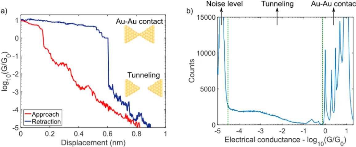
Figure 2.2: Charge transport through gold atomic contacts. a) Single opening/closing trace. b) 1D electrical histograms showing peaks at multiples of the electrical conductance quantum G0.
If more than one channel is available, all with transmission probability equal to unity, the overall conductance will be given by adding the contributions of each channel, namely G0:
G= 2e2
h ·N =N ·G0 (2.10)
where N is the number of conducting modes. Therefore, the conductance of a perfect ballistic conductor is quantized in multiples of G0. This represents a simplified version of the Landauer-Büttiker formula, because it assumes that all the conductive channels have perfect transmission. A more general formulation is found by inserting the scatterer in the 1D conductor, i.e. by supposing that some electrons can be backscattered or lose energy:
G= 2e2 h
N
X
i,j
Tij (2.11)
where Tij represents the probability that an electron passes from theithmode of the left reservoir to thejth mode of the right reservoir [15].
2.1.1 Conductance Quantization in Metallic Quantum Point Contacts
Conductance quantization can be measured by controlling the number of channels available for the electrical conduction in a 1D system. This can be achieved by shifting the Fermi level EF of the system with the help of a gate voltage, or by tuning the system size, in order to change the energy spacing between the sub-bands.
Experimental demonstrations of conductance quantization have been reported on several systems from 2D electron gases in semiconductor heterostructures [20], InAs nanowires [21] and metallic quantum point contacts.
The energy splitting between the channels is linked to the Fermi wavelength by the following relation:
∆E = π2¯h2 2m∗λF
(2.12)
2.1 Charge Transport
Since, in semiconductors λF can be of several tens of nanometers, the energy difference between the modes is on the order of few meV and conductance quantization is not observable at room temperature3. Therefore, cryogenic temperatures are usually needed to visualize the effects of quantum confinement in 2D electron gases. On the other hand, for metalsλF is much smaller (< 1 nm) and
∆E can be of the order of 1 eV. Thus, conductance quantization can be measured also at room temperature in atom-size metallic contacts [22, 23].
Charge transport in metallic quantum point contacts has been mainly studied via the so called break junction techniques, namely Mechanically Controlled Break Junction (MCBJ) and Scanning Tunneling Microscope-Break Junction (STM-BJ) [15, 24]. The latter will be briefly introduced in this section, as one of the main building blocks of the experimental technique developed during the PhD project and described in chapter 3.
The STM-Break Junction method consists in the repeated formation and breaking of contacts between the tip of a STM microscope and a metallic surface.
The electrical conductance of atom sized contacts of many different metals has been studied since the nineties with this technique [25, 22, 15], with gold being the most characterized and understood material. Also for this reason, gold was selected as the material of choice in most of the experiments reported in this work, 5 and 4.
Figure 2.2a shows a typical closing and opening trace obtained by moving the gold STM tip into contact with a gold surface while measuring the electrical current at a small fixed bias (V∼100 mV)4. During the approaching cycle (red curve), when the tip is few Å away from the surface, tunneling of electrons is recorded showing a typical exponential decay. For convenience, the electrical conductance has been plotted on a logarithmic scale and normalized with the conductance quantum G0. The tip is then approached until a Au-Au contact is formed. While opening of the junction (blue curve) the electrical conductance decreases in a step-like fashion because of conductance quantization. Right before going into the tunneling regime, a plateau at 1 G0 is typically observed, indicating the formation of a single atom contact. In fact, a single gold atom provides one electron channel for conduction with perfect transmission (T = 1). This phenomenon is very well established and it has been confirmed both experimentally and theoretically by several independent groups [15]. Especially at low temperature, long (>0.3 nm) plateaus at G0can be measured, corresponding to the formation of monoatomic chains [26, 27]. As the dynamics of the breaking process is not under experimental control, it is common practice to build one dimensional (1D) electrical histograms of few thousands opening traces5 to obtain statistically relevant information about the charge transport properties, as shown in Figure 2.2b. In the contact regime (G>1 G0), sharp peaks at multiples of the quantum of conductance appear, indicating the availability of an integer number of electronic channels and confirming that conductance quantization comes into play.
In fact, the measurement of plateaus or peaks in the histograms may be related to the plastic stages of deformation of the atomic contacts and not to conductance quantization. In gold contacts, conductance quantization typically occurs up to 3
3At T = 300 K, the average thermal energy KBT is about 26 meV, larger than the energy distance between the modes.
4Note that similar traces can be measured both at room and cryogenic temperatures.
5Closing traces are rarely used, because the high diffusivity of gold at room temperature typically hinders the formation of stable single atom contacts; typically a jump to contact is observed, as shown in Figure 2.2a.
2.1 Charge Transport
-2 -1 0 1 2 3 4
-6 -4 -2 0
log 10(T el)
Au Au
eV LUMO
HOMO
E - EF (eV)
LUMO HOMO
Off-resonance tunneling Vacuum level
a)
b)
e-
Figure 2.3: Charge transport through a single molecule. a) Energy diagram of a molecule between two metal leads, in which a positive voltage V has been applied to the right electrode. The molecular energy levels (HOMO and LUMO) are broadened because of the coupling with the metals electrodes. b) Example of electronic transmission function of HOMO dominated charge transport through a single molecule.
As a common practice, the origin of the energy scale is placed at the predicted Fermi energy EFof the junction.
G0. At larger contact sizes, multiple channels with transmissions lower than one participate to transport, breaking the quantization regime [28].
One interesting feature of the electrical conductance of atomic contacts is that the number of available channels for transport depends on the outer chemical orbitals [29]. For instance, monovalent metals like Au exhibit a single electronic channel with perfect transmission, while 5d metals like Pt feature up to 5 channels in single atom contacts, with transmission than unity giving a total electrical conductance between 1.5 and 2 G0 [30].
2.1.2 Molecular Junctions
Charge transport through molecular junctions has been widely studied in the past 20 years in the field of molecular electronics. In this section, we would like to
2.1 Charge Transport
briefly review the main concepts of charge transport which serves to understand the experiments presented in chapter 5. To get more insights into the topic, one can refer to the many books and reviews available in the literature [31, 32, 24, 33, 34].
An isolated molecule can be thought as a quantum dot, characterized by discrete energy levels and a certain HOMO-LUMO gap (representing respectively the Highest Occupied Molecular Orbital and the Lowest Unoccupied Molecular Orbital)6. When the metal-molecule-metal junction is formed, the energy levels of the molecule are broadened by the coupling with the metal electrodes, as schematically shown in Figure 2.3a. This coupling derives from the hybridization of the molecular orbitals with the continuous energy bands of the metal electrode [32]. The higher the coupling, the larger the broadening of the energy levels, and so the ability to inject charges into the molecule. Moreover, to reach the equilibrium state (constant Fermi level throughout the junction), charge transfer from the molecule to the metal electrodes or vice versa occurs, introducing a shift in the energy levels because of the additional charging energy.
The electrical conductance of the molecular junctions can be calculated from the Landauer current formula 2.7 dependent on the transmission functionτ(E). A typical electronic transmission curve is presented in Figure 2.3b. This can be obtained with Non Equilibrium Green’s Function (NEGF) methods applied to the hamiltonian of the junction, which is previously relaxed with Density Functional Theory (DFT) [18].
The peaks in the transmission are located at the energies of the molecular orbitals and their width is proportional to the coupling to the electrodes. If electrons in the contacts have energies corresponding to one of the molecular orbitals, then resonant tunneling takes place withτ = 1. This condition is hard to achieve in experiments without electrical gating of the molecular junction. Typically, the Fermi energy of the system lies in the HOMO-LUMO gap and off-resonant elastic tunneling is the main transport mechanism in short molecules (< 3 nm). For longer molecular chains instead, the tunneling contribution becomes negligible and inelastic hopping, in which electron transport is mediated via thermal vibrations, takes over [35].
As one can see from the transmission function in Figure 2.3b, the position of the Fermi energy determines the charge transport properties of the molecular junction.
In fact, in the case T = 0 K, from equation 2.7 we can calculate the electrical conductance
G= 2e2
h τ(EF) (2.13)
whereτ(EF) represents the value of the transmission function at the Fermi energy.
This stems from the fact that at T = 0 K and at small voltages the difference between the Fermi distributions of the leads can be approximated as a delta function. However, the position of the Fermi energy in the junction is typically unknown and cannot be precisely predicted with DFT methods. This results in general in bad agreement between theory and experiments on the exact value of the electrical conductance of the molecule and it is a well-known limitation of DFT.
Moreover, good agreement is usually achieved in the inter-comparison between similar molecular systems. Finally, we would like to point out that the anchoring group of the molecule (atomic group binding to the metal electrodes) usually determines if the junction is HOMO or LUMO conducting (EF closer to the HOMO
6The HOMO can be thought as the maximum of the valence band and the LUMO as the minimum of the conduction band of an equivalent semiconductor.
2.1 Charge Transport
0 0.5 1
Displacement (nm) -6
-5 -4 -3 -2 -1 0 1
log 10(G el/G 0)
0 50 100 150
-6 -5 -4 -3 -2 -1 0 1
log10(Gel/G0) 0
2000 4000 6000 8000 10000 12000
Counts
0 0.2 0.4 0.6 0.8 1
Displacement (nm) -6
-5 -4 -3 -2 -1 0 1
log 10(G/G 0)
I)
II)
III)
IV)
V)
VI) II
I
V
VI
III IV
a)
c)
b)
d)
Figure 2.4: Charge transport through a single molecule with the BJ technique. a) Example of single opening trace, showing a conductance plateau at about 10−4 G0, indicating the formation of a molecular junction. b) Elongation stages of a molecular junctions. c) 1D electrical histogram built with 5000 traces showing a clear molecular peak at 2×10⁻⁴ G0. d) 2D histogram of the electrical versus distance curves, showing that most of the opening traces exhibit molecular conductance plateaus of about 0.5 nm in the conductance region between 10−3 and 10−4 G0.
or LUMO respectively). For instance S based binding groups generally show a HOMO conducting character, corresponding to hole transport, while pyridine anchors are LUMO conducting [36, 37]. As we shall see, this determines the sign of the Seebeck coefficient of the molecular junction.
Break-Junction technique
Similar to what described for the case of gold atomic contacts in 2.1.1, charge transport in single molecule junctions has been largely studied with break-junction techniques [24]. The main advantage of this technique is that experimentally is relatively simple (in case of STM-BJ, it basically only requires a piezoelectric scanner to move the tip perpendicularly to the substrate) and it can be adapted to almost any environment from solvents [38] to UHV at cryogenic temperatures [39].
In a typical STM-BJ measurement, molecules are deposited on a metallic surface (usually gold) to form a sparse monolayer. The STM tip is then used to form and break metallic contacts with the substrate repeatedly to collect statistics. While
2.1 Charge Transport
opening the metallic junction decorated with molecules, there is a certain probability that tunneling through the molecule is measured, giving a very different signature with respect to tunneling through the empty gap. Figure 2.4a-b show a typical opening trace of the electrical conductance versus tip displacement exhibiting a plateau in correspondence to the sliding motion of the molecule in between the two gold electrodes [40]. After collecting few thousands opening traces, 1D electrical histograms can be built to extract the most probable conductance of the molecule as indicated by the peak at G < 1 G0, Figure 2.4c. Note that in the case of bare Au-Au junctions, the histogram shown in Figure 2.2b did not show any particular feature in the tunneling regime7. Another important tool, is the 2D histogram of the electrical conductance versus displacement, Figure 2.4d. To build this graphs, every opening trace is rescaled according to the breaking point of the Au-Au contacts (end of the 1 G0 plateau), so that traces with different lengths can be analyzed.
Therefore, the Au-Au contact and molecular regimes will appear at respectively negative and positive displacements. The results plotted in the 2D histograms are generally more robust against unexpected variations of the tip-surface contact. In fact, peaks in the 1D electrical histograms can also arise from contaminated opening traces (continuous traces showing long range instabilities), which could hide the characteristic signature of the molecule. Typically, the size of the accumulation region in the 2D histogram is proportional to the length of the molecule, but usually shorter because of the so called snap-back of the electrodes (plastic relaxation of the tip-shaped electrodes after breaking the Au-Au contact).
2.1.3 Electronic thermal transport and thermoelectric effects The electronic contribution to the thermal conductance in atomic and molecular junctions can also be described within the Landauer formalism [18]. In particular, if a temperature difference ∆T is imposed to the leads (TL > TR in Figure 2.1), thermal transport and thermoelectric effects come into play. In the linear regime, the currentI and heat flux ˙Q are related to the temperature difference ∆T and the voltage difference ∆V by the following relation [41, 42]:
I Q˙
!
= G L
M K
! ∆V
∆T
!
(2.14) One can then define the Seebeck coefficientS as
S= ∆V
∆T
I=0
=−L/G (2.15)
and the thermal conductancek k=− Q˙
∆T
!
I=0
=−K−S2GT (2.16)
where the minus sign in the definition of the thermal conductance takes into account the heat flux direction. Within the Landauer-Büttiker formalism, these coefficients depend on the transmission function τ(E) in the form:
7As the histograms are built with logarithmically sized bins, one expects a flat distribution for pure exponential tunneling decay
2.2 Phonon Transport
G=−2e2 h
Z +∞
0
dE∂f
∂Eτ(E) (2.17)
L=−2e2 h
kB e
Z +∞
0
dE∂f
∂Eτ(E)(E−EF)/kBT (2.18) K
T = 2e2 h
kB e
2Z +∞
0
dE∂f
∂Eτ(E)[(E−EF)/kBT]2 (2.19) wherekB is the Boltzmann constant. These integrals can be simplified with the Sommerfeld expansion if the transmission function τ(E) varies slowly on the scale ofkBT around the Fermi energy EF. In this case one finds
K ≈ −2e2
h T L0τ(EF) (2.20)
and
G≈ 2e2
h τ(EF) (2.21)
where T is the temperature of the system and L0 = keBπ32 = 2.44 V2/K2 the Lorenz number. Therefore, if S2 << L0 the electronic thermal conductance is proportional to the electrical conductance via the Wiedemann-Franz law
k≈L0T G (2.22)
Finally, the Seebeck coefficientS is proportional to the slope of the transmission functionτ(E) with the relation
S ≈ −L0eT
d lnτ(E) dE
(2.23) From these equations, we can expect that in metallic contact, the electronic contribution to the thermal conductance will be proportional to the electrical conductance, since the transmission function τ(E) is usually flat for a wide energy range aroundEF. This however does not take into account the phonon contribution, which in the case of coherent ballistic transport may increase its relative weight compared to the bulk metal. In the case of molecular junctions, we can expect the validity of the Wiedemann-Franz law, only if the Fermi energy sits far from resonances.
2.2 Phonon Transport
Thermal transport across molecular junctions is typically dominated by phonons because of their poor thermal conductance. To date, because of the lack of suitable experimental techniques, the heat transport properties of organic molecules have been mostly studied theoretically. The few experimental studies available have been focused on the properties of self assembled monolayers (SAMs) of alkane chains, because of the need of forming high quality films. A comparison between the theoretical results obtained with Molecular Dynamics (MD) simulations and ab- initio methods and the experimental results on SAMs is provided in section 5.5.
2.2 Phonon Transport
0 1 2 3 4 5
density of states
ω (THz)
hot cold
Au molecule Au
0 5 10 15 20
0 0.5
1 1.5 T ph
(meV)
a)
b) Phonon transmission
TH TC
Figure 2.5: Phonon transport through a single molecule. a) Schematic diagram of the vibrational modes of a molecule in between two gold electrodes at different temperatures, characterized by their respective phonon density of states and Bose- Einstein distribution at temperature TL,R. b) Phononic transmission function. The energy is cut off at about 20 meV, in correspondence with the Debye frequency of the gold electrodes.
The discussion about the phonon contribution to the thermal conductance of gold atomic contacts can be found in section 4.1.1. Here, we would like to outline the main features of phonon transport across single molecule junctions within the Landauer formalism.
Figure 2.5 depicts the transport model for a molecule in contact with two electrodes at different temperatures. The thermal conductance kph of this junction can be expressed with a Landauer-type of formula
kph(T) = 1 2π
Z ∞ 0
¯hωτph(ω)∂fBE(ω, T)
∂T dω (2.24)
2.2 Phonon Transport
where fBE(ω, T) = (e¯hω/kBT −1)−1 is Bose–Einstein distribution function, ¯h is reduced Planck’s constant,kBis Boltzmann’s constant andτph(ω) is the generalized phonon transmission function, containing also the coupling to the leads and the density of states of the leads. In analogy with the charge transport model presented above, the molecular junction can be viewed as a scatterer that filters the vibrational modes of the leads. The main difference from electron transport is set by the Bose- Einstein statistics: transport properties are not determined by the position of the Fermi energy (which does not exist for bosons), but all the occupied modes in the energy spectrum participate to transport and have to be considered in the calculation of the thermal conductance. Figure 2.5b shows an example of phonon transmission for a molecule between gold electrodes, calculated with a combination of DFT and Green’s function scattering methods [14, 18]. The peaks in the transmission can go above unity because they consider the 3 phonon polarization in the 3D space.
Moreover, the transmission goes to zero at about 20 meV, as this corresponds to the limit of phonon density of states in the gold electrodes. All the molecular modes at higher energies are filtered by the leads and cannot contribute to the transport properties. Therefore, the measured thermal conductance strongly depends on the choice of the leads. In general, the lighter the metal used, the higher the Debye frequency and hence the higher the thermal conductance of the junction. It is also possible to play with the mismatch in the phonon frequencies of the electrodes by using different metals to reduce the overall thermal conductance, as demonstrated in a recent experiment [9].
Another important factor influencing the heat transport properties of molecular junctions is the coupling strength to the electrodes. This is probably the most studied and understood phenomenon in these systems. By changing the binding chemistry of the molecule to the electrodes from covalent to van der Waals, reductions up to a factor of 2 have been reported [8, 43, 44]. These results stress even further the influence of interfaces in determining the heat transport properties of these nanoscale systems.
One of the most universal results that was obtained from the Landauer formula is thermal conductance quantization [45, 46, 47, 48]. In the linear regime with ∆T T and if we assume perfect coupling of the phonon modes in the electrodes with the 1D system, equation 2.24 simplifies to
k= π2kB2T
3h (2.25)
This quantum of thermal conductance represents the maximum energy that each phonon mode can carry and interestingly, it was demonstrated that it is not dependent on the particle statistics and it is valid for both bosons and fermions[49]. Quantization of thermal conductance for phonons was proved only once experimentally[50], mainly due to technical challenges involved in such heat transport measurements.
Chapter 3
Experimental Setup
In this chapter the experimental setup developed to measure the thermal properties of atomic and molecular junctions will be presented. The first section introduces the experimental technique and the basic measurement procedure. It continues with the description of the setup, the laboratory environment, the data acquisition system and the mathematical model used to calculate the thermal and electrical conductance of the junctions from the measured signals. The following section describes the design, fabrication and characterization of the MEMS sensors. Finally, the sample and tip preparation are presented in detail, starting from the surface cleaning methods of the MEMS to its surface functionalization with organic molecules and fabrication of STM tips by electrochemical etching. The fabrication of the MEMS structures is performed by our collaborator Ute Drechsler in the cleanroom at IBM Zürich.
3.1 Experimental Setup
3.1.1 Introduction
Since the invention of the Scanning Tunneling Microscope (STM) in 1981 by Gerd Binnig and Heinrich Rohrer (at IBM Zürich)[51], many research groups started investigating the physical properties of organic molecules on metallic and insulating surfaces. In addition to the imaging capabilities with atomic resolution, STM provided a way to probe charge transport in single molecules. In the late nineties, researchers started to explore systematically such charge transport phenomena, giving rise to the field of molecular electronics. The original idea of using a single molecule as electronic device is often attributed to Aviram and Ratner in 1974 [52], who proposed a molecular diode consisting of a donor and an acceptor π-system separated by a sigma-bonded tunneling bridge, predicting its rectifying characteristics. The experimental challenge of contacting a single molecule was solved by the introduction of two techniques, namely the STM-Break Junction (STM-BJ) and the Mechanically Controlled Break Junction (MCBJ)[24], see section 2.1. The basic idea of both techniques consists in dynamically forming a sub-nm gap between two metal electrodes on which the target molecules are previously deposited. While opening/closing the gap between the electrodes in the tunneling regime, there is a certain probability for one or few molecules to bridge this gap. Since the molecule can bind in many different configurations to
3.1 Experimental Setup
V4P
+
_
A
IH
VH
TH
TAMB
20μm a)
d) c)
b)
Au platform
Pt heater Suspension beam
Membrane Au tip
VBias
ISTM
+
_
A
RS
TAMB
TH1
TAMB
TH2
Qj TAMB
TAMB
TAMB
TH1
GMEMS Gj GMEMS Gj
TAMB
TH2
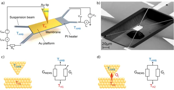
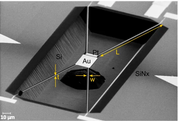
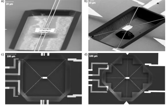
Figure 3.1: Working principle of the measurement technique. a) Schematic diagram of the experiment. To monitor the temperature TH of the gold electrode, the four-probe voltage, V4P, and the heater current, IH, are measured. Simultaneous measurement of the tunneling current, Istm, allows us to extract the electrical conductance of the junction. An external resistor Rs limits the current. b) Scanning electron micrograph of a typical MEMS used in this work. c) Prior to contact formation, the membrane is heated to TH1. The total thermal conductance of the system is given only by the contribution of the suspension beams of the MEMS. d) After contact formation, the temperature of the membrane decreases to TH2, because of the additional heat path. The total thermal conductance is now given by the sum of the thermal conductance of the MEMS (Gmems) and that of the tip-MEMS junction (Gj).
the metal electrodes, it is necessary to collect many of these conductance versus distance traces in order to get the most probable electrical conductance [53].
This break-junction method demonstrated to be very powerful to study charge transport in single molecule junctions and it was then further adapted to investigate the mechanical, optoelectronic and thermolectric properties [54]. However, heat transport in molecular systems has still been largely unexplored because of the lack of suitable experimental techniques [6]. In the following sections, I am going to explain how we combined the break junction technique with MEMS heat flux sensors to measure heat transport in single atomic and molecular junctions.
3.1.2 Working principle
In order to measure heat transport at the atomic and molecular scale, we combined the STM-BJ technique with highly thermally insulated heat flux sensors consisting of a suspended Micro-Electro Mechanical System (MEMS) with an integrated micro- heater, Figure 3.1. The experiments are performed in high vacuum (10−7 mbar) and at room temperature with a custom-built STM setup located in the IBM Noise Free Labs [55]. With the STM-BJ technique, we can measure the electrical conductance of the tip-MEMS contact and understand whether we have a single atom or a single molecule in the junction. The electrical conductance represents our reference signal, and thanks to the progress made in the molecular electronics field, we can use it to
3.1 Experimental Setup
get information about the structure of the molecular/atomic junctions [56].
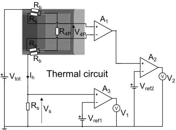
The MEMS consists of 4 SiNx suspension beams connected to a central part, which features a Pt micro-heater, to control and monitor the temperature, and a metallic platform, to form electrical contacts with the STM tip. Thermal equilibrium is assumed between the platform and the heater, due to larger thermal resistance of the suspension beams.The tip and the metallic platform are usually made out of gold, as one of the most commonly used metal in molecular electronics. To obtain the thermal conductance of the junction, we heat the MEMS to a temperature TH by applying a constant voltage to the heater and then measure the heat flux to the tip, at room temperature, while forming and breaking contacts. Prior to contact formation, heat can be transported from the MEMS to the substrate only through the suspension beams1. We can then calculate the thermal conductance of the MEMS, defined as
Gmems= Q˙
∆T (3.1)
where ˙Q is the total power provided by Joule dissipation and ∆T is the resulting temperature difference. Once a contact between the tip and the gold platform is formed, the ∆T decreases because of the additional heat path. In the electronic analogy, one can translate this scenario to the parallel of two conductances, as tip and substrate are at the same temperature. The thermal conductance of the junction is then obtained by subtracting the previously measured Gmems. Typically, this procedure is repeated few 1000s times to collect statistics as in a standard break-junction measurement.
From this brief explanation, 2 important aspects of the measurement can already be understood:
1. To obtain the thermal conductance of the tip-MEMS contact we have to subtract a reference value, which, in the simplest case, corresponds to the thermal conductance of the MEMS, Gmems. This means that the amplitude of the measured temperature change depends on the ratio between Gmemsand Gj; hence to have a good signal to noise ratio, the MEMS sensors should feature a thermal resistance as close as possible to Gj.
2. To finely control the breaking process of the junction, the MEMS has to be mechanically stiff, setting a trade-off between mechanical stability and heat flux sensitivity.
In the following sections, these aspects will be addressed in some detail, as they provide the guidelines to design the experiment.
3.1.3 The setup
The development of the experimental setup, was initiated by Dr. Bernd Gotsmann.
When I joined IBM in 2014, I started by optimizing, programming and developing the system further to reach the sensitivity needed for measuring the thermal conductance of single molecular junctions. The setup consists fundamentally of
1Note that in high vacuum there is no heat conduction through air. Moreover, the contribution of radiation to the thermal conductance of the MEMS is negligible for the temperature differences (<100 K) set during the experiment.
3.1 Experimental Setup
Ion Pump
Turbo Pump Pressure Gauges
Gate Valve High-vacuum
chamber ADwin
ANC150 SR640
SR640 ANC250
Tip holder xyz-scanner
xy-positioners
Sample
MEMS Probecard
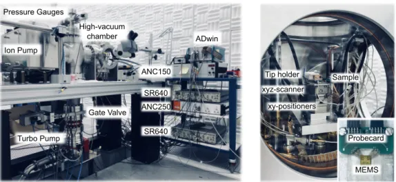
Figure 3.2: Picture of the experimental setup in the Noise Free Labs at IBM Zurich. On the left, one can see most of the setup and the sensitive electronic instruments. On the right, a view of the interior of the vacuum chamber with the piezo-scanner and positioners is shown. The inset displays a MEMS sensor (5 x 5 mm) electrically connected to the probecard on the sample holder.
a custom-built scanning tunneling microscope (STM) in high-vacuum, Figure 3.2. It is placed on an optical table, which is fixed on the concrete block of the anti-vibration system of the lab. The turbo pump (HiPaceR 300 from Pfeiffer Vacuum) is connected to the main vacuum chamber from the bottom through a flexible hose to damp the vibrations generated by the rotation of the pump blades.
The exhaust of the turbo pump is connected to the rotary pump located in the auxiliary room of the lab to reduce the noise. A pneumatic gate valve (VAT) can be used to isolate the vacuum chamber, so that the turbo pump can be switched-off. In this case, to maintain the low pressure inside the chamber, the ion pump (TiTanR from Gamma Vacuum) connected to the left side of the chamber is turned on. This combination allows us to minimize the mechanical vibrations induced on the setup while performing an experiment. We can reach a vacuum level below 10−6 mbar within an hour, if the chamber was not left to ambient pressure for more than a couple of hours. To increase the lifetime of the ion pump, we typically wait for the pressure to be around 10−7 mbar, which can take up to 12 hours. The chamber features 6 openings connected via CF160 flanges. A quick access door on the front allows us to load the sample and exchange tips. All the vacuum parts, apart from the door, are UHV compatible to allow more flexibility for the future developments of the setup. Inside the chamber (Figure 3.2), the sample holder is placed on a stack of piezoelectric elements consisting of 2 positioners (Attocube ANPx101) for the coarse motion in-plane and the open loop xyz-scanner (Attocube ANSxyz100) to perform STM-break junction measurements or STM imaging. The holder consists of a stainless steel base plate on top of which a probecard (from SQC AG) with pins arranged in a fixed layout is mounted. The MEMS samples are designed with the same contact layout, so that samples can be quickly exchanged without the need of wafer bonding. The holder is then magnetically fixed on the scanner thanks an intermediate plate screwed on the scanner itself which contains few strong permanent magnets. The tip holder is placed in front of the piezo-stack on the
3.1 Experimental Setup
100 μm
Figure 3.3: SEM image of a MEMS sampleOn the right side, the Au pad used to perform break junction tests is visible. On the left side, the MEMS is indicated by two arrow-like structures that serve for the optical positioning of the tip onto the gold platform.
positioner for the out-of-plane motion (Attocube ANPz101), which is used to coarse approach the tip to the sample surface. The lower piezoelectric elements are screwed on an aluminum base plate, which is suspended via 4 VitonR O-rings to damp the mechanical vibrations coming especially from the turbo pump. This simple solution is quite effective and it allows us to perform the break junction experiments with the pump running. In fact, it is very convenient to start measurements and perform preliminary tests on new samples while the turbo pump is still running, as one can save 5-10 hours of pumping time. The position of the aluminum plate inside the setup is adjusted at few cm distance from the front door, to enable optical access to the sample via the stereo-microscope. This is aspect is very important, because it allows us to reposition the tip on the MEMS anytime during the experiment or to move it to the substrate. It is in fact normal practice in the STM community to clean or reshape the tip, by gently crashing it onto a metallic surface with a high voltage applied (>5 V). As this step cannot be performed directly on the MEMS, mainly because of induced overheating, we typically move the tip to the substrate and do such tests on a predefined gold pad, as shown in Figure 3.3.
One last important aspect of the setup is the cabling inside the vacuum chamber.
To minimize the electronic noise level of the measured signals, it is better to use short coaxial cables directly from the probecard to the feedthroughs. At the same time, the cables mechanically link the piezo-scanner with the chamber, and thus their stiffness must be also minimized. Therefore, we decided to connect the probecard to an intermediate series of pins, which are fixed on the aluminum baseplate and connected to the feedthroughs via longer coaxial cables.
3.1.4 Noise Free Labs
The setup is located in the Binnig-Roher Nanotechnology center in Zurich inside one of the Noise Free Labs. These laboratories were devised in order to reduce the influence of external noise sources so that almost any kind of experiment would profit from such an environment. The laboratory consists of an experiment room where the setup and the sensitive electronic equipments are placed, one operator room, from where the researcher can control the setup and two additional side rooms, containing the noisy equipments like the scroll pump for the pre-vacuum and the PC
3.1 Experimental Setup
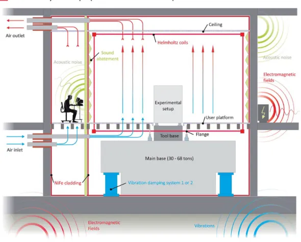
Figure 3.4: Schematic of the laboratory concept. The laboratory combines air conditioning system for the humidity and temperature control, shields and active compensation to screen external electromagnetic fields and vibration isolation, achieving unprecedented low levels for the main noise sources (reproduced from [57],[55]).
itself. Figure 3.4 shows a cross-section of the lab with the operator and experiment room. The setup is placed on a large concrete block of 30 to 68 tons to passively damp the high frequency mechanical vibrations (above 5 Hz). This main base is further suspended on a combination of air springs and air cushions to allow for active compensation of the remaining vibrations. With this implementation, vibrations of less than 300 nm/s at 1 Hz and less than 10 nm/s above 100 Hz were achieved. The air conditioning system was designed in a way that the air flow does not excite the concrete block. In this way, the temperature is kept constant within ±0.01 ◦C and the humidity within±2%. Sound-absorbing panels cover the walls of the experiment room to absorb the acoustic noise generated inside and outside of the laboratory.
Isotropically conducting NiFe sheets (80% Ni, 20% Fe) were used to coat the door, walls and ceiling, forming a magnetic cage that shields from mid and low frequency electro-magnetic fields (100 Hz – 100 kHz). An aluminum top layer was welded to the magnetic layer forming a Faraday cage. Moreover, three Helmholtz coils were installed inside the room to actively compensate for variations in the DC magnetic field. In terms of performances, electromagnetic fields with AC peaks of less than 0.3 nT at 50 Hz and 250 Hz and DC variations of less than±15 nT were achieved.
Working in such a special environment, particular care has to be taken in order to not
3.1 Experimental Setup
DAC ADC
ANC250
ANC150 Switch
Box
SR640 differential
amplifier
IV converter
SR640 differential
amplifier
STM circuit
Piezo-scanner
Thermal circuit
Xs Ys Zs
Xp Yp Zp
Coarse positioners
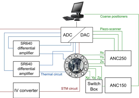
Figure 3.5: Schematic view of the data acquisition and control circuitry.
The red circuit is used to measure the tunneling current between the STM tip and the MEMS platform. The green circuit controls the piezoelectric scanner through the high-voltage amplifier ANC250 and the coarse positioners through the ANC150 control unit. Finally, the blue circuit is used to measure the 4-probe resistance of the heater element integrated on the MEMS and the dissipated electrical power.
degrade the performances of the laboratory and profit the most from it. For instance, we tried to damp the vibrations coming from the vacuum pumps by using flexible vacuum connectors to the the main chamber. Despite of generating electric noise, we placed most of the electronic instruments (differential amplifiers and ADC/DAC cards) inside the laboratory close to the experiments, to minimize the pick-up noise induced in long coaxial cables and the input capacitances to the amplifiers. Even if we cannot directly measure the benefits of being in this controlled environment for our experiment, we definitely observe great advantages, compared to a standard laboratory. First of all, thanks to the vibration damping system and the temperature stabilization, mechanical drifts of the piezoelectric positioners/scanner are greatly minimized. Moreover, keeping continuously a constant temperature greatly reduces the variations in the electronic offsets and gains of the amplifiers. For instance the voltage offsets at open circuit that we measure before starting every experiment show very small variations from month to month.
3.1.5 Data acquisition and system control
The data acquisition system is depicted in Figure 3.5. The measurement unit is the ADwin Pro II, featuring an internal processing unit with 300 MHz clock rate, 768 kB local memory and 256 MB RAM which allows floating point operations with