Elektro(nik)geräte
Inverse Production Line for the Automated Dismantling of Mobile Phones with Selective Laser-based Detaching
and Sorting of Valuable Components
Reinhard Noll, Sven Connemann, Cord Fricke-Begemann, Frederik Schreckenberg, Roland Ambrosch, Alice Tori and Marco Guolo
1. The project next generation urban mining – automated disassembly, separation and recovery
of valuable materials from electronic equipment (ADIR) ...534
2. Disassembly and extraction of printed circuit board (PCB) ...535
3. Measuring geometric and chemical features of PCBs ...537
4. Unsoldering and sorting ...540
5. Conclusion ...542
6. References ...543
Increasing masses of electronic consumer goods are flooding modern societies. In these products a variety of valuable substances are bound covering more and more elements of the periodic system. Examples of such products are mobile phones and printed circuit boards (PCB) from personal computers and servers. So far, for their recycling conventional mass stream treatment techniques are deployed as, e.g., shred- ding, sorting of the shredder output and metallurgical refining to recover copper and precious metals. However, shredding is a more or less unspecific destructive technique with high energy consumption to generate as output a material mixture characterised by a range of grain sizes but also by a high entropy. Shredding generates intrinsically disorder and dust. Thus physically well separated components of the incoming material stream are crushed and mixed. By this process approach some valuable materials are lost in dust or in slag fractions of the subsequent metallurgical treatment.
A cornerstone for an efficient circular economy is to overcome these limitations of conventional mass treatment by efficient and selective physical separation of valuable components from these end-of-life products. Instead of generating disorder, a process has to be conceived to keep and even increase the order in terms of selective dismantling of valuable components and their sorting to specifically enriched material fractions.
Modern production and laser technologies – so far applied only to manufacture new products – allow for this approach which is denoted here as inverse production.
Elektro(nik)geräte
1. The project next generation urban mining – automated disassembly, separation and recovery of valuable materials from electronic equipment (ADIR)
A European consortium has launched the project ADIR in September 2015 to develop and to set-up for the first time an inverse production line for end-of-life (EOL) mobile phones (MPH) and large PCBs from personal computers and servers [1]. ADIR covers the whole process chain from the collection of EOL-electronics, via singularisation, feeding, robotic handling, measuring, dismantling, sorting up to the metallurgical treatment of the sorted fractions with pyro- and hydro-metallurgical processes [3].
The involved partners are: Fraunhofer Institute for Laser Technology (ILT), Aachen, Germany; Pro Automation GmbH, Vienna, Austria; H.C. Starck GmbH (HCS), Goslar, Germany; Instytut Metali Niezelaznych (IMN), Gliwice, Poland; Aurubis AG (AU), Lünen, Germany; Laser Analytical Systems & Automation GmbH (LSA), Aachen, Germany; Osai Automation Systems S.p.A. (OS), Parella, Italy; Electrocycling GmbH (ECG), Goslar, Germany; Tre Tau Engineering srl (TRT), Torino, Italy.
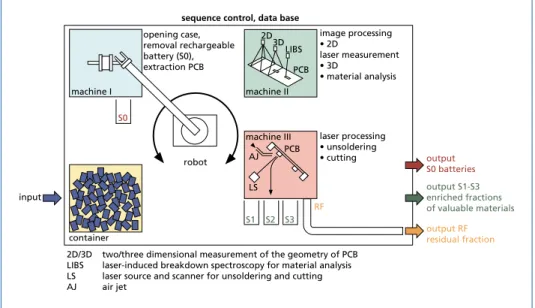
In this contribution we report about the actual status of the R&D achievements for the three main processes and machines constituting the inverse production line of the ADIR demonstrator, here stated for the case of mobile phones: I) mechanical picking, opening of housing, extraction of battery, separation of PCB, passing on of PCB to subsequent machine; II) measuring of PCB: 2D/3D geometry and chemical composition, building up a data base; III) selective unsoldering and sorting of electronic components from the PCB. Figure 1 illustrates these processes and the respective machines I to III [5].
Figure 1: Concept of the ADIR demonstrator; a robot and a manipulator are picking single ob- jects from the input stream and feed sequentially the machines I, II and III for selective disassembly of mobile phones and printed circuit boards (PCB)
sequence control, data base opening case,
removal rechargeable battery (S0), extraction PCB
S0
S1 S2 S3
machine I machine II
machine III
AJ PCB
RF PCB 3DLIBS 2D
LS
container
output S0 batteries output S1-S3 enriched fractions of valuable materials input
output RF residual fraction 2D/3D two/three dimensional measurement of the geometry of PCB
LIBS laser-induced breakdown spectroscopy for material analysis LS laser source and scanner for unsoldering and cutting AJ air jet
robot
image processing
• 2D
laser measurement
• 3D
• material analysis
laser processing
• unsoldering
• cutting
Elektro(nik)geräte
The collected end-of-life mobile phones are piled in a container and fed to a conveyor (not shown in Figure 1). A robot equipped with a camera is picking a single object and positions this piece in a first machine (I), where the case of the MPH is opened, the rechargeable battery is removed and put into bin S0 (sorting fraction zero). The printed circuit board is taken out from machine I and a manipulator transfers this PCB to the next machine (II). Machine II performs various measurements at the PCB. It takes 2D and 3D (by laser) images, processes these to identify interesting components potentially containing high amounts of valuable material. A laser spectroscopic measurement based on LIBS (laser-induced breakdown spectroscopy) measures inline constituents of these components, as e.g. tantalum [2]. These data are used to feed a data base and to extract coordinates for the laser beam control to unsolder components from the PCB or to cut out parts of that PCB in machine III.
The measured object is transferred from machine II to machine III where the identified components are selectively unsoldered or cut out from the PCB. The disassembled com- ponents are discharged to the sorting fractions S1 to S3. After removal of the selected components the residual object goes to a residual fraction (RF).
The ADIR demonstrator yields, e.g., five output streams: a) sorted fraction S0 contai- ning rechargeable batteries (output of machine I), b) sorted fractions S1 to S3 with high-content of target materials from selectively disassembled components (output of machine III), c) residual fraction RF (output of machines I and III). These fractions, especially S1 to S3, are studied for efficient recovery of valuable materials by the involved R&D institute of non-ferrous metals research (IMN), the electro-recycling company (ECG) and two metal and semi-finished products manufacturers (HCS, AU).
In the following sections we describe the status of the processes and machines I (PA), II (ILT, LSA) and III (OS).
2. Disassembly and extraction of printed circuit board (PCB)
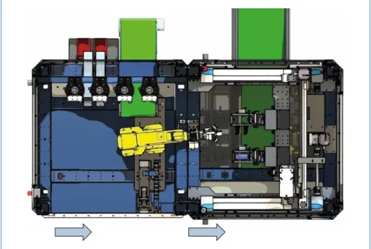
Figure 2 shows the concept of machine I for the mechanical dismantling process of mobile phones consisting of two robot cells. In this machine, the incoming mobile phones are dismantled and separated into different parts for subsequent processing in machines II and III (grey arrow at the bottom right). In the first step – before the objects reach machine I – the mobile phones are unloaded onto a feeding conveyor belt from a special bunker and are then transferred to machine I (grey arrow at the bottom left). The mobile phones are detected by a camera mounted above the feeding conveyor belt (not shown in Figure 2) in order to obtain the information about the type of the mobile phone, its position and orientation.
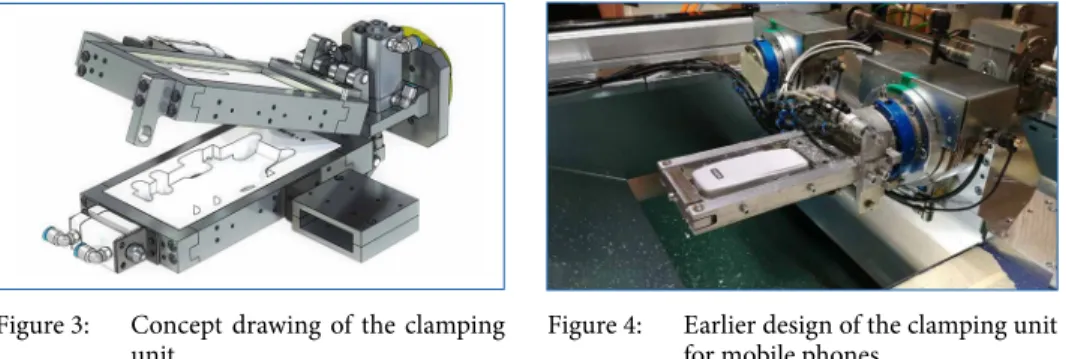
The robot in the cell picks up the object from the belt and places it into one of the two clamping units (at the right half of Figure 2). One clamping unit is designed for mobile phones, while another is intended for larger PCB, e.g., from computers. The clamping unit concept has been revised several times, due to various technical challenges such as the instability of the casing of mobile phones during the disassembly process. The newly developed clamping system (Figure 3), ensures robust and flexible clamping of
Elektro(nik)geräte
the object during mechanical processing. It is mounted on a slew unit that can rotate in the required direction and additionally allows for a quick manual change of the entire unit, thus considering potential future changes in the requirements for the processed material.
Figure 2: Machine I, view from the top; robot (yellow); overall process flow direction of the objects to be treated: grey arrows; at the top the various output streams of machine I are located:
chutes/bins/belt conveyors
A milling unit disintegrates the housing of the MPH and allows access to the inner con- stituents. At this stage, mobile phones are processed according to specific instructions developed for particular mobile phone models. These instructions include all robot positions, speed, movement type, picking, all milling positions, all clamping unit actions and more. The convenience of this approach allows for future alteration only within the instructions, rather than the complete software. Once the milling is finished successfully, the gained parts such as batteries, speakers, vibration alerts and loudspeakers are sorted into the designated sorting fractions (at the upper part of the sketch shown in Figure 2).
The extraction process has been also disturbed by a number of technical issues that required further analyses. Mainly the challenges have been associated with the earlier design of the clamping unit (Figure 4) and the respective instructions used for dismant- ling. Thus, one of the main challenges pertaining to the battery liberation concerns the mobile phone instability resulting in an inefficient battery removal. During the tests the battery clamps could not be removed reliably, the battery was jammed in the mobile phone housing, or the battery could not be picked up, because the mobile phone was
Elektro(nik)geräte
pushed through the clamping unit. The unsatisfying reliability of the clamping unit resulted in the mobile phone losing its position and/or the ultimate damage thereof.
Hence, the abovementioned clamping mechanism has been developed to ensure process robustness and, additionally, increase process safety.
Figure 3: Concept drawing of the clamping
unit Figure 4: Earlier design of the clamping unit
for mobile phones
After extraction, the PCB of the mobile phone is placed in a second clamping unit that ensures its stability for the removal of the metal shielding (radio frequency shielding).
The metal shielding is milled off the PCB to allow access to the relevant valuable com- ponents mounted on the PCB for the processes of machines II and III. The liberated PCBs are eventually taken out of machine I for further processing (grey arrow at the bottom, right in Figure 2).
The PCBs are transported between the machines by means of an automated manipu- lator that consists of a gantry robot. This robot is equipped with two grippers, one for the PCBs extracted from mobile phones, while another one for the larger PCBs from computer and server stations. The manipulator connects all three machines and moves the PCB between them along the complete line. The manipulator picks the PCB, trans- ports it to the next machine and places it in a special drawer of that machine which is then pulled in prior to the subsequent processing step.
The automated system functions without human intervention, which is required only at the stage of the initial MPH or PCB feeding and replacing of the filled sorting bins with extracted constituents.
3. Measuring geometric and chemical features of PCBs
The complete description of the design of PCBs including the chemical composition of the used electronic components is not provided by the manufacturers. However, this knowledge is a mandatory prerequisite for a selective disassembly. Machine II is designed to perform an optical inspection of PCBs to provide this physical and che- mical information.
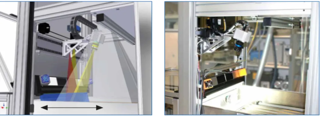
Machine II combines measurements by 2D and 3D cameras with laser spectroscopic material identification. The concept of the machine and the set-up during the instal- lation phase is shown in Figure 5.
Elektro(nik)geräte
Figure 5: Concept of machine II; beam paths of the 2D and 3D cameras (left); realised optical set-up (right); the black double arrow at the left image shows the direction of movement of the measuring object during the measurements
The PCBs are positioned by the manipulator in a drawer of machine II where the PCBs are fixed and moved to the interior of the machine. After completion of the measure- ments, the drawer opens again and the PCB is picked again by the manipulator and automatically transferred to machine III.
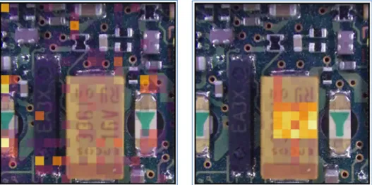
Colour images of each PCB are taken with a spatial resolution of about 50 µm to enable the identification of components down to below 1 mm in size as well as production marks on the PCB. Using an image processing software, a list of all components on the PCB can be determined. An example for a PCB from a mobile phone is shown in Figure 6. In parallel, laser light section images are acquired to obtain 3D data from the PCB surface. A laser line is projected onto the surface and imaged by a camera. The triangulation method is used to determine the surface height at each position, thus a 3D image is generated. From this image, additional information is derived to identify electronic components and also to check the accessibility of individual components on the PCB. Based on the list of components mounted on the PCB and the information gathered in the data base, it is determined which components are of possible interest for extraction and need to be analysed chemically.
The chemical analysis is carried out using laser-induced breakdown spectroscopy, LIBS [4]. Each location to be investigated is irradiated by a pulsed laser beam using an optical scanner to guide the beam to the selected measuring location. The non- contact laser method performs two process steps. First, the surface material, e.g., the housing of the components, is ablated locally to provide access to the material in the core of the components. Subsequently the core material is excited by the laser pulses and element specific optical emissions are detected which reveal the elements used to build the components.
As an example, the right-hand picture in Figure 6 shows the result of a scan of the PCB at a fixed raster of 2 mm step size. For each position the intensity of emissions origi- nating from tantalum is evaluated and depicted in a false colour map highlighting the positions with a high tantalum content. Some components become clearly visible as tantalum capacitors when comparing the chemical map (right) with the 2D image (left).
Elektro(nik)geräte
Since this example used a full-size scan of the PCB with a fixed step size, small compo- nents can be missed. Therefore, the practical application will more specifically analyse individual components identified prior by the image processing.
To demonstrate the spatial resolution of the LIBS measurements, Figure 7 shows a scan in the area of a SMD (surface mounted device) component having a size of a few millimetres. The step size of the scanning laser beam is reduced to 0.5 mm. The left-hand picture shows an overlay of the 2D image with the LIBS map for tantalum measured directly at the surface level, where no clear signals are visible. In contrast, the right-hand picture shows the overlay with the LIBS map obtained after ablation of the surface material. Prior exposures have revealed the material in a depth of about 1 mm, where the LIBS measurements now clearly provide a signature for tantalum.
High tantalum content is found in the centre region of the SMD component where the tantalum containing anode block of the capacitor is located. Measurements outside this region show elements used to construct other internal parts of the component. Since the spectroscopic measurement is a multi-element analysis, all elements of interest for recycling are detected simultaneously without increase of the measurement time.
The findings of the LIBS analysis for each component investigated on the PCB are fed into the data base. Based on the requirements of the metallurgical recycling processes, this information about chemical compositions is used to determine which components are extracted selectively for separate processing and to which sorting fraction they will be assigned. This data is deployed for the selective laser detachment of components from a PCB in machine III.
Figure 6:
2D image of a PCB from a mo- bile phone, size: 109 x 42 mm2 (left); false colour plot of loca- tions identified by laser spectros- copy where a significant amount of tantalum is present (right, step size of raster scan for laser spectroscopy: 2 mm)
Elektro(nik)geräte
4. Unsoldering and sorting
Machine III is dedicated to unsoldering and cutting actions based on the information gained in machine II. Figure 8 shows the realised set-up of this machine.
Figure 7: Detailed raster scan of the components marked by the white square in Figure 6, left (size about 10 x 10 mm2); overlay of 2D image with chemical information (coloured squares) indicating tantalum if only a single laser pulse train is irradiated per measuring location (left); consecutive raster scans yielding chemical information from a depth of about 1 mm after ablation of surface layers (right)
Figure 8: Front view of machine III, in the opening the manipulator will put the PCB to be processed (left); backside of machine III with exit ports for various sorting and residual fractions (right) The overall machine dimensions are 2,000 x 3,000 x 2,300 (height) mm3, thus allowing to process not only PCBs from MPHs but also large PCBs from computers and servers with dimensions of up to 520 x 520 mm2 within a laser processing area of 750 x 750 mm2.
Elektro(nik)geräte
The configuration of the machine permits to process PCBs with different thicknes- ses, shapes and dimensions, thus allowing a standard and universal approach. The laser source is an ytterbium fibre laser. The laser emits at wavelengths near 1,070 nm and yields a total radiant flux of light at the optical output of about 1,000 Watts. Dedica- ted chiller and fume extractor have been designed and positioned close to the machine.
The extraction of components, once unsoldered or cut out, has been realised through an ad hoc tool (under patent app- lication). The extraction tool consists in a multimaterial suction nozzle, realised with flexible material, and an air blow pipe with a precise conformation. The suction nozzle and the air blow pipe are mounted on a rotational z-axis, thus allowing the free approaching to the components to be extracted. This specific configuration guarantees to approach and extract the components at 360°. The suction nozzle has been designed and realised using a multimaterial concept to prevent the collision with components and to avoid the breakage of the suction nozzle itself.
The machine III concept includes a dra- wer for the loading of the PCBs by the manipulator and a conveyor belt for the discharging of the residual fractions after selective extraction of the valuable elec- tronic components.
A universal clamping system has been designed for the correct positioning and clamping of the PCBs during any phase of the process. The clamping concept consists of a load plane on which the manipulator positions the PCB as shown in Figure 9.
The PCBs are properly fixed for the laser process thanks to the alignment of two parallel bars as shown in Figure 10.
Figure 9: Loading and clamping of a PCB in machine III; the arrow shows the loaded PCB of a mobile phone
Figure 10: Clamped PCB; PCB from a mobile phone (top); clamped PCB from a server (bottom, dimensions 370 x 500 mm2)
Elektro(nik)geräte
Figure 11:
Drawer with sorting fractions unsoldered or cut out automati- cally from PCBs
The components detached are collected in specific boxes according to their composi- tion, e.g.: S1a – Ta containing components, except from surface acoustic wave (SAW) filters; S1b – SAW filters; S2 – W containing components; S3 – Nd containing com- ponents and S4 – further elements (future definition). The sorting fraction boxes and collection tools have been installed in machine III, both for unsoldered and cut out components (Figure 11).
Machine III has been designed for the interconnection with machines I and II and for the communication with the general data base. Sorting order rules have been identi- fied. A dedicated software for the functioning of the machine has been developed and standardised both for PCBs from mobile phones and for large PCBs from computers and servers to control unsoldering and cut out actions.
The average time to unsolder and to sort a SMD is < 2 s. The cutting speed for a typical PCB board amounts to about 50 cm/min.
5. Conclusion
Within the European project ADIR new technologies are explored to enable an effici- ent urban mining by deploying novel inverse production schemes. Treated items are end-of-life mobile phones and printed circuit boards from computers and servers. The goal is to physically separate components of these products containing highly enriched
Elektro(nik)geräte
contents of valuable materials. The elementary processes for feeding singularised items, automatic disassembly, 2D/3D measurement, laser spectroscopic analysis, laser unsol- dering and cutting were worked out and their capability was checked successfully in laboratory scale. During the course of 2018 the described machines will be integrated to the ADIR demonstrator and then be tested in field tests at a recycling plant (ECG) to validate the capability of an automatic disassembly, separation and recovery of valuable materials from electronic equipment.
Acknowledgement The authors wish to express their thanks to the European Union, represented by the European Commission, for enabling the project ADIR. This project has received funding from the European Union’s Horizon 2020 research and innovation programme under grant agreement No 680449. Furthermore, the authors of Fraunhofer ILT thank the Fraunhofer society for the provided cofinancing means.
6. References
[1] ADIR project website: http://www.ADIR.eu
[2] Fricke-Begemann, C.; Connemann, S.; Schreckenberg, F.; Noll, R.: LIBS for identification and localization of valuable materials in electronic waste, Paper presented at the EMSLIBS2017 &
CSI XL conference, Pisa, June 2017
[3] Noll, R.; Ambrosch, R.; Bergmann, K.; Britten, S.; Brumm, H.; Chmielarz, A.; Connemann, S.;
Eschen, M.; Frank, A.; Fricke-Begemann, C.; Gehlen, C.; Gorewoda, T.; Guolo, M.; Kurylak, W.;
Makowe, J.; Sellin, G.; Siguier, M.; Tori, A.; Veglia, F.: Next generation urban mining – automated disassembly, separation and recovery of valuable materials from electronic equipment: overview of R&D approaches and first results of the European project ADIR, Proc. Europ. Metallurgical Conf. EMC 2017, pp. 799-816
[4] Noll, R.: Laser-induced breakdown spectroscopy – Fundamentals and applications. Heidelberg:
Springer-Verlag, 2012, p. 543
[5] Patent of Fraunhofer Society, DE 10 2011 012 592, 15.10.2015
Dorfstraße 51
D-16816 Nietwerder-Neuruppin
Tel. +49.3391-45.45-0 • Fax +49.3391-45.45-10 E-Mail: tkverlag@vivis.de
Bestellen Sie direkt beim TK Verlag oder unter www. .de
TK Verlag GmbH
Michael Beckmann K. J. Thomé-Kozmiensky
DEZENTRALE ENERGIEVERSORGUNG DEZENTRALE ENERGIEVERSORGUNG
Erneuerbare Energien und
Dezentrale Energieversorgung
Erneuerbare Energien, Band 1 bis 6 Dezentrale Energieversorgung
Paketpreis 90,00 EUR
statt 140,00 EUR Erneuerbare Energien, Band 1 (2009) ISBN: 978-3-935317-44-3 20,00 EUR
Erneuerbare Energien, Band 4 (2010) ISBN: 978-3-935317-55-9 20,00 EUR Erneuerbare Energien, Band 5 (2011) ISBN: 978-3-935317-64-1 20,00 EUR Erneuerbare Energien, Band 6 (2011) ISBN: 978-3-935317-65-8 20,00 EUR Erneuerbare Energien, Band 2 (2009) ISBN: 978-3-935317-43-6 20,00 EUR Erneuerbare Energien, Band 3 (2010) ISBN: 978-3-935317-54-2 20,00 EUR
Dezentrale Energieversorgung (2013) ISBN: 978-3-935317-95-5 20,00 EUR Herausgeber: Karl J. Thomé-Kozmiensky und Michael Beckmann • Verlag: TK Verlag Karl Thomé-Kozmiensky
Die Deutsche Nationalbibliothek verzeichnet diese Publikation in der Deutschen Nationalbibliografie; detaillierte bibliografische Daten sind im Internet über http://dnb.dnb.de abrufbar
Stephanie Thiel • Elisabeth Thomé-Kozmiensky • Daniel Goldmann (Hrsg.):
Recycling und Rohstoffe – Band 11
ISBN 978-3-944310-40-4 Thomé-Kozmiensky Verlag GmbH
Copyright: Elisabeth Thomé-Kozmiensky, M.Sc., Dr.-Ing. Stephanie Thiel Alle Rechte vorbehalten
Verlag: Thomé-Kozmiensky Verlag GmbH • Neuruppin 2018
Redaktion und Lektorat: Dr.-Ing. Stephanie Thiel, Dr.-Ing. Olaf Holm, Elisabeth Thomé-Kozmiensky, M.Sc.
Erfassung und Layout: Claudia Naumann-Deppe, Janin Burbott-Seidel, Sandra Peters, Ginette Teske, Cordula Müller, Gabi Spiegel
Druck: Universal Medien GmbH, München
Dieses Werk ist urheberrechtlich geschützt. Die dadurch begründeten Rechte, insbesondere die der Übersetzung, des Nachdrucks, des Vortrags, der Entnahme von Abbildungen und Tabellen, der Funk- sendung, der Mikroverfilmung oder der Vervielfältigung auf anderen Wegen und der Speicherung in Datenverarbeitungsanlagen, bleiben, auch bei nur auszugsweiser Verwertung, vorbehalten. Eine Vervielfältigung dieses Werkes oder von Teilen dieses Werkes ist auch im Einzelfall nur in den Grenzen der gesetzlichen Bestimmungen des Urheberrechtsgesetzes der Bundesrepublik Deutschland vom 9.
September 1965 in der jeweils geltenden Fassung zulässig. Sie ist grundsätzlich vergütungspflichtig.
Zuwiderhandlungen unterliegen den Strafbestimmungen des Urheberrechtsgesetzes.
Die Wiedergabe von Gebrauchsnamen, Handelsnamen, Warenbezeichnungen usw. in diesem Werk berechtigt auch ohne besondere Kennzeichnung nicht zu der Annahme, dass solche Namen im Sinne der Warenzeichen- und Markenschutz-Gesetzgebung als frei zu betrachten wären und daher von jedermann benutzt werden dürfen.
Sollte in diesem Werk direkt oder indirekt auf Gesetze, Vorschriften oder Richtlinien, z.B. DIN, VDI, VDE, VGB Bezug genommen oder aus ihnen zitiert worden sein, so kann der Verlag keine Gewähr für Richtigkeit, Vollständigkeit oder Aktualität übernehmen. Es empfiehlt sich, gegebenenfalls für die eigenen Arbeiten die vollständigen Vorschriften oder Richtlinien in der jeweils gültigen Fassung hinzuzuziehen.