VLSI Design Concepts for Iterative Algorithms
Von der Fakult¨ at f¨ ur Elektrotechnik und Informationstechnik der Technischen Universit¨ at Dortmund
genehmigte Dissertation
zur Erlangung des akademischen Grades Doktor der Ingenieurwissenschaften
eingereicht von Chi-Chia Sun
Tag der m¨ undlichen Pr¨ ufung: 11.04.2011
Hauptreferent: Univ.-Prof. Dr.-Ing. J¨ urgen G¨ otze Korreferent: Univ.-Prof. Dr.-Ing. R¨ udiger Kays
Arbeitsgebiet Datentechnik, Technische Universit¨ at Dortmund
Abstract
Circuit design becomes more and more complicated, especially when the Very Large Scale Integration (VLSI) manufacturing technology node keeps shrinking down to nanoscale level. New challenges come up such as an increasing gap between the design productivity and the Moore’s Law. Leakage power becomes a major factor of the power consumption and traditional shared bus transmission is the critical bottleneck in the billion transistors Multi-Processor System–on–Chip (MPSoC) designs.
These issues lead us to discuss the impact on the design of iterative algorithms.
This thesis presents several strategies that satisfy various design con- straints, which can be used to explore superior solutions for the circuit design of iterative algorithms. Four selected examples of iterative al- gorithms are elaborated in this respect: hardware implementation of COordinate Rotation DIgital Computer (CORDIC) processor for sig- nal processing, configurable DCT and integer transformations based CORDIC algorithm for image/video compression, parallel Jacobi Eigen- value Decomposition (EVD) method with arbitrary iterations for com- munication, and acceleration of parallel Sparse Matrix–Vector Multipli- cation (SMVM) operations based Network–on–Chip (NoC) for solving systems of linear equations. These four applications of iterative meth- ods have been chosen since they cover a wide area of current signal processing tasks.
Each method has its own unique design criteria when it comes to the direct implementation on the circuit level. Therefore, a balanced solution between various design tradeoffs is elaborated for each method.
These tradeoffs are between throughput and power consumption, com-
putational complexity and transformation accuracy, the number of in-
ner/outer iterations and energy consumption, data structure and net-
work topology. It is shown that all of these algorithms can be imple-
mented on FPGA devices or as ASICs efficiently.
Acknowledgements
This thesis was written while I was working as a research assistant at the Information Processing Laboratory of the Dortmund University of Tech- nology. I would like to thank Professor Dr.-Ing. J¨ urgen G¨otze, the head of the laboratory, for all the interesting discussions that contributed es- sentially to this thesis, for creating an open and relaxed atmosphere, and for providing excellent working conditions.
Furthermore, I am very pleased to thank Professor Dr.-Ing. R¨ udiger Kays (TU Dortmund) for his interest in my works, his comments on my thesis and his reviews for my DAAD scholarship, and his time.
I would also like to thank Professor Shanq-Jang Ruan (Low-Power System Lab, National Taiwan University of Science and Technology) for his guidance during my Master study in Taipei. I am especially grateful to my present and former colleagues for providing such a stimulating atmosphere at the laboratory. It was a pleasure to share so much time with you. Special thanks goes to many students for their contributions to this work too.
To my parents and my sister for their support and encouragements during the long years of my education.
Dortmund Germany, April 2011
Contents
1 Introduction 1
2 Introduction to VLSI Design 9
2.1 Modern Digital Circuit Design . . . . 9
2.2 Moore’s Law . . . 11
2.3 Circuit Design Issues: Modular Design . . . 12
2.4 Circuit Design Issues: Low Power . . . 16
2.5 Circuit Design Issues: Synthesis for Power Efficiency . . 17
2.6 Circuit Design Issues: Source of Power Dissipation . . . . 19
2.6.1 Dynamic Power Dissipation . . . 20
2.6.2 Short Circuit Power Dissipation . . . 21
2.6.3 Static Leakage Power Dissipation . . . 21
2.7 Design Consideration for Iterative Algorithms . . . 23
2.8 Summary . . . 24
3 CORDIC Algorithm 25 3.1 Generic CORDIC Algorithm . . . 25
3.2 Extension to Linear and Hyperbolic functions . . . 30
3.3 CORDIC in Hardware . . . 32
3.4 Hardware Performance Analysis . . . 35
3.5 Summary . . . 36
4 Discrete Cosine Integer Transform (DCIT) 37 4.1 Introduction of DCIT . . . 37
4.2 DCT algorithms . . . 39
4.2.1 The DCT Background . . . 39
4.2.2 The CORDIC based Loeffler DCT . . . 40
4.2.3 4 × 4 Integer Transform . . . 42
4.2.4 8 × 8 Integer Transform . . . 43
4.3 Discrete Cosine and Integer Transform . . . 46
4.3.1 Forward DCIT . . . 46
4.3.2 Inverse DCIT . . . 48
4.4.2 The CORDIC based Scaler . . . 53
4.4.3 The CORDIC-Scaler Configurator and the LUT Read Module . . . 57
4.4.4 The Post-Quantizer . . . 61
4.5 Experimental Results . . . 63
4.5.1 Variable Iteration Steps of CORDIC . . . 64
4.5.2 ASIC Implementation . . . 65
4.5.3 Performance in MPEG–4 XVID and H.264 . . . . 67
4.6 Summary . . . 75
5 Parallel Jacobi Algorithm 77 5.1 Parallel Eigenvalue Decomposition . . . 78
5.1.1 Jacobi Method . . . 78
5.1.2 Jacobi EVD Array . . . 79
5.2 Architecture Consideration . . . 81
5.2.1 Conventional CORDIC Solution . . . 81
5.2.2 Simplified µ–rotation CORDIC . . . 83
5.2.3 Adaptive µ–CORDIC iterations . . . 85
5.2.4 Exchanging inner and outer iterations . . . 86
5.3 Experimental Results . . . 87
5.3.1 Matlab Simulation . . . 87
5.3.2 Using threshold methods . . . 89
5.3.3 Configurable Jacobi EVD Array . . . 91
5.3.4 Circuit Implementation . . . 94
5.4 Summary . . . 98
6 Sparse Matrix–Vector Multiplication on Network–on–Chip 101 6.1 Introduction of Sparse Matrix–Vector Multiplication . . . 102
6.2 SMVM on Network-on-Chip . . . 103
6.2.1 Sparse Matrix-Vector Multiplication . . . 103
6.2.2 Conjugate Gradient Solver . . . 105
6.2.3 Basic Idea . . . 106
6.3 Implementation . . . 108
6.3.1 Packet Format . . . 108
6.3.2 Switch Architecture . . . 109
6.3.3 Pipelined Switch Architecture . . . 111
6.3.4 Routing Algorithm . . . 112
6.3.5 Processing Element . . . 113
6.3.6 Data Mapping . . . 113
6.4 Experimental Result . . . 115
6.4.1 FPGA Implementation . . . 115
6.4.2 Influence of the Sparsity . . . 116
6.4.3 Mapping to Iterative Solver . . . 118
6.5 Summary . . . 120
7 Conclusions 121
A Appendix Tables 125
B Appendix Figures 129
Bibliography 137
List of Figures
1.1 Designer productivity gap (modified from SEMATECH) 2 1.2 Iterative algorithm design concept . . . . 3 2.1 Moore’s Law: Plot of x86 CPU transistor counts from
1970 until 2010 . . . 11 2.2 IC scaling roadmap for More than Moore (modified figure
from 2009 International Technology Roadmap for Semi-
conductors Executive Summary) [58] . . . 13 2.3 Relative delays of interconnection wire and gate in nanoscale
level (regenerated figure from International Technology
Roadmap for Semiconductors 2003) [57] . . . 14 2.4 The prediction of future multi-core SoC performance (re-
generated figure from 2009 International Technology Roadmap for Semiconductors System Drivers) [59] . . . 15 2.5 A typical NoC architecture with a mesh style packet-
switched network . . . 16 2.6 Power reduction at each design level [88] . . . 18 2.7 A simple CMOS inverter . . . 20 2.8 There are four components of leakage sources in NMOS:
Subthreshold leakage (I Sub ), Gate-oxide leakage (I Gate ), Reverse biased junction leakage (I Rev ) and Gate Induced
Drain Leakage (I GIDL ) . . . 22 3.1 CORDIC rotating and scaling a input vector < x 0 , y 0 >
in the orthogonal rotation mode . . . 28 3.2 CORDIC rotating a input vector < x 0 , y 0 > in the or-
thogonal vector mode . . . 29 3.3 Flow graph of a folded CORDIC (recursive) processor . . 33 3.4 Flow graph of an unfolded (parallel) CORDIC processor 34 3.5 Flow graph of an unfolded (parallel) CORDIC processor
with pipelining . . . 34
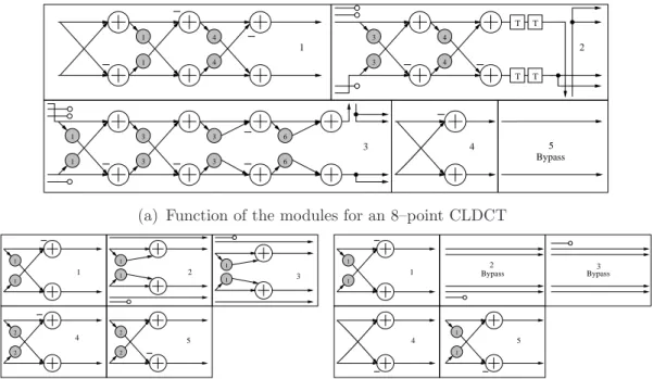
4.1 Flow graph of an 8–point Loeffler DCT architecture . . . 41
4.3 Flow graph of the 4–point integer transform in H.264 . . 44 4.4 Flow graph of the 8–point integer transform in H.264 . . 46 4.5 Flow graph of an 8–point FDCIT Transform with five
configurable modules for multiplierless DCT and integer
transforms [106] . . . 47 4.6 Three sub flow graphs of the modules of Figure 4.5 . . . 48 4.7 Flow graph of an 8–point IDCIT Transform with seven
configurable modules for multiplierless IDCT and inverse
integer transforms . . . 49 4.8 Three sub flow graphs of the modules of Figure 4.7 . . . 50 4.9 The framework of the proposed CORDIC based 2-D FQD-
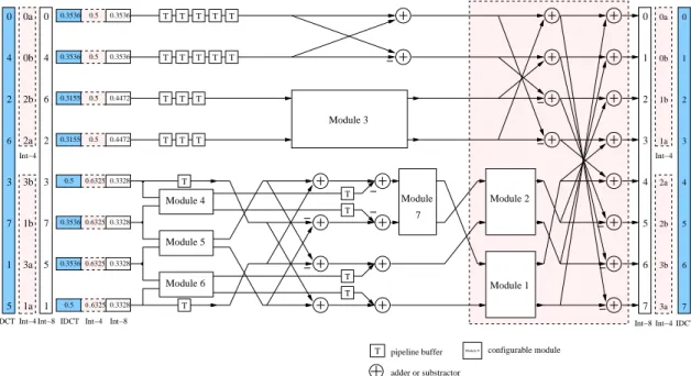
CIT with four CORDIC-Scalers, a Post-Quantizer, a CORDIC- Scaler Configurator, a LookUp Table Read Module and
17 dedicated LUTs (8 are for DCT and the other 9 are
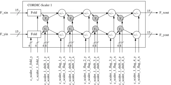
for integer transforms) . . . 52 4.10 Framework of a CORDIC based 2-D IQDCIT . . . 53 4.11 Schematic view of the first CORDIC-Scaler with one Fold
and four CORDIC compensation steps . . . 54 4.12 Schematic view and IOs of the LUT reader module and
CORDIC-Scaler configurator module . . . 60 4.13 Schematic view of the Post-Quantizer . . . 62 4.14 Three flow graphs of CORDIC-Scaler with different num-
ber of CORDIC compensation steps . . . 65 4.15 Final layout view of the 2–D CORDIC based FQDCIT
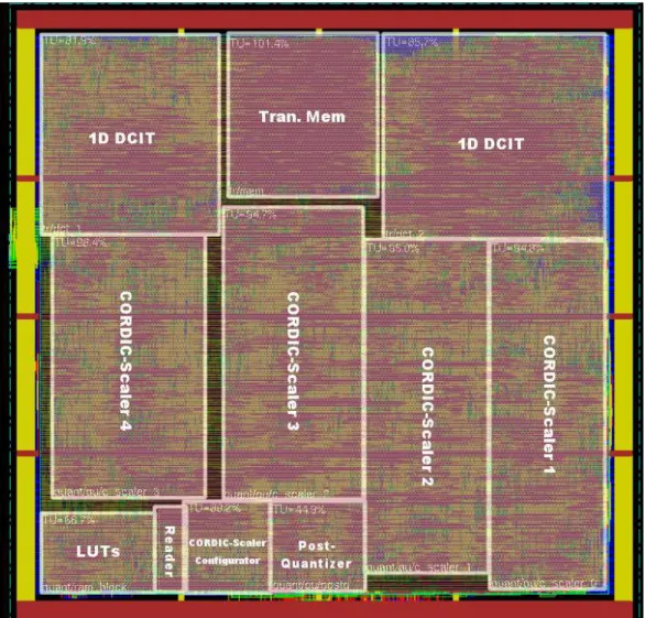
implementation in TSMC 0.18µm technology library . . 66 4.16 Timing waveform of the 2–D CORDIC based FQDCIT
in the DCT mode (requiring 29 clock cycles for latency) . 68 4.17 The average Forward Q+DCT, FNQDCT and FQDCIT
PSNR of the “foreman” and “paris” cif video test from
low to high bitrates in XVID . . . 71 4.18 The average FQDCIT PSNR of the “foreman” and “paris”
cif video test from low to high bitrates in H.264 . . . 71 4.19 The average IQDCIT PSNR of the “foreman”, “paris”
and “news” cif video test from low to high bitrates in
XVID . . . 72 4.20 The average IQDCIT PSNR of the “crew” and “ice”
DVD video test from low to high bitrates in XVID . . . 73
4.21 The average IQDCIT PSNR of the “rush hour” and “blue
sky” Full–HD video test from low to high bitrates in XVID 73 4.22 The average IQDCIT PSNR of the “foreman”, “paris”
and “news” cif video test from low to high bitrates in
H.264 . . . 74 4.23 The average IQDCIT PSNR of the “crew” and “ice”
DVD video test from low to high bitrates in H.264 . . . . 75 4.24 The average IQDCIT PSNR of the “rush hour” and “blue
sky” Full–HD video test from low to high bitrates in H.264 76 5.1 A 4 × 4 EVD array, where n=8 for 8 × 8 symmetric matrix 80 5.2 Flow graph of a folded CORDIC (recursive) processor
with the scaling . . . 83 5.3 Four simplified CORDIC rotation types . . . 84 5.4 The block diagram of a scaling–free µ–CORDIC PE, in-
cluding 2 adders, 2 shifters and 4 multiplexers . . . 86 5.5 The average number of sweeps vs. array sizes for four
rotation methods (µ–CORDIC, Full CORDIC and two
adaptive methods). . . 87 5.6 The number of shift–add operations for four rotation
methods on different size of array . . . 89 5.7 The required number of sweeps vs. off–diagonal norm for
10 × 10 Jacobi EVD array with double floating precision . 90 5.8 The required number of sweeps vs. off–diagonal norm for
80 × 80 Jacobi EVD array with double floating precision . 91 5.9 The required number of sweeps vs. off–diagonal norm for
10 × 10 Jacobi EVD array with single floating precision . 92 5.10 The required number of sweeps vs. off–diagonal norm for
80 × 80 Jacobi EVD array with single floating precision . 93 5.11 The reduction of shift–add operations (in percent) for
three rotation methods with the threshold strategy and preconditioned E index on different size of array in IEEE
754 single floating precision . . . 94 5.12 3–D bar statistic view of the l = E − 127 index for adap-
tive index selection for 10 × 10 Jacobi EVD array with
single floating precision . . . 95 5.13 3–D bar statistic view of the l = E − 127 index for adap-
tive index selection for 80 × 80 Jacobi EVD array with
single floating precision . . . 95
5.15 A configurable parallel Jacobi EVD design . . . 96
5.16 Final layout view of a 10 × 10 Jacobi EVD array with the µ–CORDIC PE with TSMC 45nm technology library. . . 97
5.17 The energy consumption per EVD operation with each size of EVD array (operating at 100 MHz) . . . 98
6.1 The quadratic surface of the f (x) . . . 105
6.2 A direct mapping of parallel SMVM operations based on the NoC architecture . . . 107
6.3 The system level view of a 4 × 4 SMVM-NoC in Xilinx Virtex–6 . . . 108
6.4 Detailed switch interconnection including two 3 × 3 cross- bars, five I/O ports and four FIFOs . . . 110
6.5 A 5–stage pipelined switch with two 3 × 3 crossbars, five I/O ports and four FIFOs . . . 112
6.6 Schematic view of the PE for the SMVM–NoC platform . 113 6.7 Performance analysis of different matrix size with ran- dom sparsity on the Pentium-4 PC, non–pipelined 4 × 4/8 × 8 SMVM-NoC, 4 × 4/8 × 8 pipelined SMVM-NoC (operat- ing at 200MHz) . . . 117
6.8 Influence of sparsity on different architectures with ran- dom sparsity from 10% to 50% . . . 118
6.9 Analysis of the packet traffics for the 4 × 4 pipelined SMVM– NoC . . . 119
6.10 Two clock regions for the PE and the switch, one for PE running at higher frequency, another lower frequency . . 120
B.1 CORDIC linear rotation mode . . . 130
B.2 CORDIC linear vector mode . . . 130
B.3 CORDIC hyperbolic rotation mode . . . 131
B.4 CORDIC hyperbolic vector mode . . . 131
B.5 Seven video sequences for test the QDCIT transformation 132
B.6 An inverse mapping of parallel SMVM operations based
on the NoC architecture . . . 132
List of Tables
2.1 Typical switching activity levels [5] . . . 21 3.1 Three different rotation types of CORDIC with both ro-
tation and vector modes used for implementing the dig- ital processing algorithms (said n iterations and rotated
with a target angle φ t ) . . . 26 3.2 Comparison of three different CORDIC dependence flow
graphs . . . 34 3.3 Implementation results of three different CORDIC de-
pendence flow graphs with the orthogonal rotation mode
in Xilinx Virtex–5 FPGA (xc5vlx110t-1ff1136) . . . 35 4.1 Control Signals for the proposed framework of 2–D QDCIT 53 4.2 The corresponding QPs of Luma DC and Chroma DC
values in MPEG-4 . . . 54 4.3 Values of QStep dependent on QP in H.264 . . . 55 4.4 LUT organization of an entry for Quantization of DCT
coefficients . . . 58 4.5 LUT organization of an entry for Quantization of 4 ×
4/8 × 8-integer transform coefficients . . . 59 4.6 Complexity for each 2-D quantized transformation archi-
tecture . . . 63 4.7 2–D Transformation Complexity for arbitrary CORDIC
iterations . . . 64 4.8 Comparison of various DCT implementations and the
proposed 2-D FQDCIT in different design criteria (area,
timing, power, latency, throughput and architecture) . . 69
4.9 The list of test sequences . . . 70
gle, the required shift–add operations for rotation and scaling, the required cycle delay and repeat numner for
CORDIC–6 [109]. . . 99 5.2 Area, Delay and Power Consumption results of 4 × 4 and
10 × 10 Jacobi EVD arrays with the TSMC 45nm tech-
nology. . . 100 6.1 Packet Format . . . 109 6.2 An example of packing vector elements and nonzero ma-
trix elements into packet format ( × denotes empty and Bold/Italic fonts denote that these packets have to be
mapped on the same PE.) . . . 114 6.3 Synthesis Results of pipelined SMVM-NoC Architecture
in Xilinx Virtex-6 (XC6VLX240T-1FF1156) . . . 116 6.4 The performance comparison between non–pipelined 4 × 4
SMVM-NoC and pipelined 4 × 4 SMVM-NoC (NZs: Nonzero Elements) . . . 116 A.1 The detailed information for each x86 based CPU from
1970 until 2010 . . . 126 A.2 The pseudo code for each type of Jacobi parallel EVD
code generation . . . 127
1 Introduction
Modern Very Large Scale Integration (VLSI) manufacturing technology has kept shrinking down to Very Deep Sub-Micron (VDSM) with a very fast trend and Moore’s Law is expected to hold for the next decade [1, 41] or extend to the More than Moore concept (a prediction for the integration of more than thousand cores before 2020) [21, 64, 95]. 10 years ago, for 0.35µm technology, design engineers focused on reducing the area size to lower down the cost. Later, when it came to 0.13µm technology, they paid huge efforts to improve the signal integrity and reduce the power consumption for low power devices. More and more functionalities can be integrated on an integrated circuit due to the continuing improvements.
As the manufacturing technology node decreases to the 65nm, the circuit design methodology poses new challenges: timing delay of the global wire interconnection is increasing severely in relation to the local processor element, leakage power becomes a major factor of the power consumption, and shared bus transmission is the new bottleneck in the billion transistors System–on–Chip (SoC) designs [24, 99, 125]. On the other hand, as product life cycle continues to shrink simultaneously, time–to–market also becomes a key design constraint. In consequence, these problems result in the famous “designer productivity gap” as il- lustrated in Figure 1.1 [85]. In this chart, the x–axis denotes the pro- gression in time and the y–axis denotes the growing rate as measured by the number of logic transistors per chip. The solid line shows the growth rate based on the Moore’s Law, while the dotted line sketches the average number of transistors that design engineers could handle monthly. It can be noticed in Figure 1.1 that there is an increasing gap.
Consequently, silicon technology is far outstripping our ability to utilize these transistors efficiently for working designs in a short time.
Several strategies have been proposed to solve this widening produc-
Design Complixity by Moore’s Law 50%
Designer Productivity 20%~25%
Designer Productivity Gap
Time
Growth Rate
Figure 1.1: Designer productivity gap (modified from SEMATECH)
tivity gap. One of the most efficient solutions is using parallel comput- ing, which has received great attention. It has been introduced in many state-of-the-art applications in the past few years (e.g. Six-Core CPU, MPSoC and parallel processor arrays) [104, 120, 121, 132]. In addition, modulized circuit design has developed to very large SoC by utilizing reusable/configurable Intellectual Property (IP) cores as much as pos- sible [17]. Soon traditional bus transmission architecture will be unable to satisfy the need for more than thousand cores on a single silicon die.
Hence, a better network switching method is desired.
These challenges motivate us to analyze their impact on parallel iter-
ative algorithms. We try to present a generalized VLSI design concept
that considers the significant impact on power, performance, cost, re-
liability, and time–to–market. To implement an iterative algorithm on
a multiprocessor array, there is a tradeoff between the complexity of
an iteration step (assuming that the convergence of the algorithm is
retained) and the number of required iteration steps. For example,
suppose we have a hardware platform with multiple processors which
requires an iteration step of the iterative algorithm to be executed K
times in order to obtain the convergence. The iteration step is exe-
cuted in parallel on the platform. We want to simplify the processors
in order to improve the logical utilization of the platform as shown in
Figure 1.2. This simplification will usually cause an increased number
of iterations for convergence. The number of required iterations will
increase from K to K + L. That means the number of data transfer in
1 Introduction 3
Hareware Platform
L K
Hareware Platform Simplified K
Figure 1.2: Iterative algorithm design concept
the interconnections also increases due to the behavior of the iterative algorithm. Therefore, as long as the convergence properties are guaran- teed, it is possible to adjust the architecture which is normally resulting in an increased number of iteration steps. This reduces the complex- ity with regard to the implementation significantly. However, it is not easy to find a superior solution to balance the design criteria, especially for the performance/complexity of the hardware, the load/throughput of interconnects and the overall energy/power consumption. An exam- ple of this in the SoC design is the area and the timing optimization.
Area is a metric that is aggressively optimized to achieve low chip cost.
In contrast, timing closure is achieved when a particular target clock frequency is met (further timing optimization is not necessary). Opti- mization of one metric can be traded off for the optimization of other one. Obviously, it is extremely difficult to optimize all metrics at the same time.
As we will emphasize throughout this thesis, a design engineer must think carefully which strategy should be selected for the hardware im- plementation of iterative algorithms. However, a proper decision be- comes more and more difficult as VLSI technology is evolving. This problem motivates us to study the design issues. Four different itera- tive algorithms have been selected, which cover a wide area of current signal processing tasks. All of them are implemented and realized in order to discuss the relationship between circuit design issues and the algorithmic complexity. The chosen algorithms are:
CORDIC processor A COordinate Rotation DIgital Computer (CORDIC)
can perform a lot of mathematical computations to accelerate many digital functions and signal processing applications in hard- ware, including linear and orthogonal transformations by requir- ing only shift and add operations. Since the CORDIC is also an important iterative algorithm, a brief introduction to the generic definition and the hardware implementation issues will be given first. It is a simple, but very flexible arithmetical unit. Very sim- ple modifications to the controller lead to linear and orthogonal operating modes, capable of calculating vector rotations, angle estimations or even multiplications/divisions. Various conditions concerning the circuit design issues will be described and com- pared, particularly on the architecture level. We elaborate the way of implementing a CORDIC rotation with reasonable com- putational complexity by trading off the throughput [6, 83].
Discrete Cosine Integer Transform (DCIT) VLSI implementation of both forward and inverse CORDIC based Quantized DCIT (QD- CIT) is presented. This configurable architecture not only per- forms multiplierless 8 × 8 Quantized DCT (QDCT) and 4 × 4/8 × 8 integer transforms but also contains configurable modules such that it can adjust the number of CORDIC rotations for arbi- trary accuracy. Therefore, the presented architecture reduces the number of iterations when the target resolution is small (QCIF/- CIF). On the contrary, it will apply more iterations when the target resolution is large (Full-HD/Ultra-HD). Moreover, it still retains an acceptable transformation quality compared to the de- fault methods in terms of PSNR. This leads to a high-accuracy high throughput implementation [106, 107, 112, 113].
Parallel Jacobi EVD method Parallel Jacobi method for Eigenvalue
Decomposition (EVD) is chosen as an example to explain the de-
sign concepts concerning tradeoff between the complexity and the
iteration (see Figure 1.2). Here, it is chosen since its convergence
property is very robust. Simplifying the hardware architecture is
paid by an increased number of rotations due to the behavior of
Jacobi’s algorithm. Nevertheless, the computational complexity is
actually decreased, which also results in lower energy consumption
per EVD operation [46, 109]. The implementation results demon-
strate that using the simplified architecture is beneficial concern-
ing the design criteria since it yields smaller area overhead, faster
1 Introduction 5 overall computation time and less energy consumption.
Sparse Matrix-Vector Multiplication based on NoC Future integra- tion of more than thousands IP cores for the very large SoC de- sign will soon challenge the current shared bus transmission sys- tem [133]. In this regard, a Sparse Matrix-Vector Multiplication (SMVM) calculator with the chip-internal network is presented as a novel solution for parallel matrix computation to further acceler- ate many iterative solvers in hardware, such as solving systems of linear equations, Finite Element Method (FEM) and so on [110].
This methodology is called Network–on–Chip (NoC). Using NoC architecture allows the parallel processors to deal with irregular structure of the sparse matrices and achieve a high performance in FPGA by trading off the area overhead, especially when the data transfers are unstable.
In this thesis, our major concern is to explore several VLSI design con- cepts for iterative algorithms. Contrary to conventional circuit designs, usually reducing the logical utilization and increasing the performance, we will further look into parallel computing, configurable architecture and packet–switched network. The goal is not to optimize one or several criteria as much as possible, but trying to expose the complete tradeoff curves and to have a global view on how large the range is for real-life applications. The major contributions of this thesis are:
1. The description of different circuit design challenges is introduced briefly, especially when the technology node is very small. This leads us further to discuss the design impact on iterative algo- rithms from the algorithmic and the architectural point of views.
2. The investigation of VLSI design concepts is presented for future circuit design in nanoscale for four selected iterative applications:
CORDIC processor for signal processing, configurable transfor-
mations for video compression, parallel EVD for communication
and parallel SMVM for solving systems of linear equations. Each
application has its own unique design criteria requiring design en-
gineers to think carefully. They require investigating the tradeoffs
between throughput and power consumption, computational com-
plexity and transformation accuracy, the number of inner/outer
iterations and energy consumption, data structure and network topology. These tradeoffs are further elaborated to obtain a bal- anced solution for each application.
3. The circuit implementations of both forward and inverse QD- CIT transformations based on the CORDIC algorithm are pre- sented. The CORDIC based FQDCIT requires only 120 adders and 40 barrel shifters to perform the multiplierless 8 × 8 FQDCT and 4 × 4/8 × 8 forward quantized integer transform by sharing the hardware resources. Hence it can support different video Codecs, such as JPEG, MPEG–4, H.264 or SVC. Furthermore, for a TSMC 0.18µm circuit implementation, it can achieve small chip area and high throughput for future UHD resolution. On the other hand, the inverse architecture requires only 124 adders and 40 barrel shifters to perform the multiplierless 8 × 8 IQDCT and quantized 4 × 4/8 × 8 inverse integer transform. Meanwhile, the ability to adjust CORDIC iteration steps can be used to support different video resolutions.
4. A configurable Jacobi EVD array has been elaborated with both Full CORDIC (exact rotation, executing W CORDIC iterations, where W is the word length) and µ–CORDIC (approximate ro- tation, executing only one CORDIC iteration) in order to further study the tradeoff between the performance/complexity of pro- cessors and the load/throughput of interconnects. Moreover, uti- lizing a preconditioned E index method not only reduces more than 35% computational overhead for the Full CORDIC and 10%
for the µ–CORDIC in average, but also omits the floating point number comparators. For a TSMC 45nm circuit implementation, a detailed comparison between area, timing delay and power/en- ergy consumption is done.
5. A solution for sparse matrix computation based on the NoC con-
cept is presented. Parallel SMVM computations have been tested
in the Xilinx Virtex–6 FPGA. The advantages of introducing the
NoC structure into SMVM computation are given by high resource
utilization, flexibility and the ability to communicate among het-
erogeneous systems. This configurable solution can be configured
as a larger p × p array as long as there are enough hardware re-
sources (p = 2, 4, 8, . . . , 2 k , k ∈ N ). Moreover, the NoC structure
1 Introduction 7 can guarantee that arbitrary sparsity structures of the matrix can be handled without interfering the performance by the sparsity of the matrix.
This thesis is organized as follows: Chapter 2 gives a brief intro-
duction to recent VLSI design trends, on the parallel implementation
issues, and the low power design methodology. Then, in Chapter 3, the
CORDIC algorithm is introduced and it is shown how it is derived and
implemented. Two typical iterative algorithms based on the CORIDC
architecture, Discrete Cosine and Integer Transform and parallel Jacobi
EVD, will be presented and tested in Chapter 4 and Chapter 5 respec-
tively. After that, in Chapter 6, SMVM based NoC is presented and
preliminary implementation results are given. Finally, conclusions are
given in Chapter 7.
2 Introduction to VLSI Design
In this chapter, a brief introduction to the future trend of VLSI design and its circuit design problems will be addressed. Moore’s Law is ex- pected to hold for at least 10 more years. Meanwhile, digital multimedia devices will keep driving the demand for very complex SoC systems. A single chip can contain more than billion transistors to support various functionalities. Therefore, before looking into the design issues of iter- ative algorithms, it is very important to review today’s nanoscale VLSI technology in Section 2.1. The reason how Moore’s Law will continue to influence the circuit design trend will be explained in Section 2.2.
Several strategies for obtaining the timing convergence and reducing the power optimization from a higher design level to the lower level will be described from Section 2.3 to Section 2.5. The power consumption of CMOS circuit and the corresponding solutions will be introduced in Section 2.6. At the end, our motivation on VLSI design concepts for iterative algorithms will be clarified in Section 2.7.
2.1 Modern Digital Circuit Design
Silicon technology is now at the stage where it is feasible to incorporate
numerous transistors on a single square centimeter of silicon such that
Intel predicts the availability of 100 billion transistors on a 300mm 2 die
in 2015 [17]. At this moment, multi-core SoC design emerged because it
allowed design engineers to integrate few cores together for simple par-
allel computing. This permits to build as a complete SoC for supporting
extremely complex functions, which would previously be implemented
as a collection of individual chips on a PCB board. Now, since the
nano-technology allows the integration of an ever-increasing number
of macro-cells on a single silicon die, parallel multiprocessor platforms
have received great attention and have been realized into several state-
of-the-art applications (e.g. Six–Core, MPSoC and parallel processor array) [8, 17, 132].
Besides the issue of parallelism, the ability to integrate all parts of applications on the same piece of silicon is also beneficial for lower power, greater reliability and reduced cost of manufacturing for con- sumer electronic devices. Consequently, increased pressure has been put on design engineers to meet a much shorter time–to–market, now measured in months rather than years. Particularly, with the new in- dustry standards such as H.264, WCDMA, and WiMAX, which keep driving the growth of High–Definition TV (HDTV) and smart phone.
However, the decreasing development period for a new Application- Specific Integrated Circuit (ASIC) not only results in a very high Non- recurring Engineering (NRE) cost, but also makes it hard to succeed the goal of time–to–market. Therefore, another popular solution Field Programmable Gate Array (FPGA) plays an important role for fitting the gap between cost and flexibility.
FPGA is an integrated circuit, which is designed to be configured
after manufacturing. The FPGA configuration is generally specified us-
ing a Hardware Description Language (HDL), similar to that used for
an ASIC design. Hence, FPGAs can be used to implement any logical
function that an ASIC can do. In this way, the capability to update
the functionality, partial reconfiguration of the design and the low NRE
costs offer advantages to many applications [134]. However, the manu-
facturing cost per FPGA still makes it unsuitable for many consumer
standard devices. For example, the price of an FPGA die which can
be configured as a video decoder with MPEG–4 decoding functionality
will be much higher than a dedicated ASIC. Therefore, the choice be-
tween the FPGA and the ASIC design is simple the question if either
the size of market is large enough to afford ASIC development costs or
the devices need the reconfiguration for supporting new functionalities
after shipping.
2.2 Moore’s Law 11
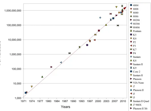
Figure 2.1: Moore’s Law: Plot of x86 CPU transistor counts from 1970 until 2010
2.2 Moore’s Law
In 1965 Gordon E. Moore has predicted a long-term trend of computing hardware, in which the number of transistors that can be placed on an integrated circuit will double approximately every two years [80]. Note that it is often incorrectly cited as a doubling of transistors every 18 months. The actual average period is about 20 months. Historically, Moore’s Law has precisely described a driving force of technological and social change with respect to cost, functionality and performance in the late 20th and early 21st centuries. For example, if we consider the CPU transistor counts from 1970 until 2010 in Figure 2.1, it results in a con- stant line corresponding to exponential growth due to the logarithmic scale.
At the beginning, the first x86 Intel 4004 contained only thousand
transistors; 10 years ago, the transistor counts of an Intel Pentium in-
creased very fast to a million transistors. Until now a single Quad-
Core/Six-Core CPU can integrate more than a billion transistors. In
Appendix A, Table A.1 shows more detailed information for each x86
CPU model. In the future, Moore’s Law will continue until 2020 [41,90]
or maybe even further. After that, soon CMOS technology will meet its physical limitation when the node size is smaller than 10nm. Now many scientists are trying to replace the current silicon based MOS- FET by a novel carbon based Carbon Nanotube Field Effect Transistor (CNFET) or spintronics in order to shrink the node size into the atom level [7, 61, 86]. If it comes true, the computer will usher in a new era
“Beyond CMOS” (also known as “More Moore”). Unfortunately, it seems that this is probably not going to happen so easily in the next 10 years. On the other hand, other groups came out with another poten- tial way to keep Moore’s Law alive by using a Three-Dimensional IC (3D-IC) concept to increase the density of transistors [66, 91]. As far as we can see the Through-Silicon Via (TSV) technology for 3D-IC will be feasible before 2012.
More and more evidences point out that the trend of Moore’s Law becomes slow, especially the 2009 executive summary of International Technology Roadmap for Semiconductors (ITRS) provides a taxonomy of scaling in the traditional, “More than Moore” sense. Figure 2.2 shows three possible trends. They envision future integrated circuit system will perform diverse functions such as high-accuracy sensing of real-time signals, energy harvesting, and on-chip chemical/biological sensors in a System-in-Package (SiP) or a System-of-Package (SoP) design [64, 95].
In this way, the incorporation of functionalities into devices will not necessarily scale according to Moore’s Law but provide additional value to the end customer in different ways. The More than Moore approach will allow for the non-digital functionalities (e.q. RF communication, power control, passive components, sensors, actuators) to migrate from the system board-level into particular SiP/SoP potential solutions [119].
So far, we still could not tell which solution will dominate the future design trend, especially there are many design issues require engineers further discuss.
2.3 Circuit Design Issues: Modular Design
Recently, the growing complexity of multi–core architectures will soon
require highly scalable communication infrastructure. Today most of
2.3 Circuit Design Issues: Modular Design 13
130nm 90nm 65nm 45nm 32nm 22nm
Analog/RF Passives Power Biochips Sensors
Very large SoC Digital content Information Processing New Standards
SiP/SoP design Interacting with people and enviroment
Non−digital content
Beyond CMOS
Moore’s Law
More than Moore
Combing SoC and SiP/SoP, Many−Core system 3D IC
Figure 2.2: IC scaling roadmap for More than Moore (modified figure from 2009 International Technology Roadmap for Semiconductors Executive Summary) [58]
the current communication architectures in multi-core SoC are still based on dedicated wiring. With shirking process technology, logic components such as gates have also decreased in size. However, the traditional wiring lengths do not shrink accordingly, resulting in rela- tively longer communication path lengths between logic components.
For instance, when the technology node is 65nm, the metal–layer wire delay is 10 times larger than the gate node delay as shown in Figure 2.3.
Moreover, the data synchronization issue with a single clock source has also become a critical problem for circuit synthesis [14,51]. That means the timing closure issue on the large SoC design is difficult to be solved.
In the meantime, design resource reuse concerns all additional activ-
ities that have to be performed to generate an easy–to–use and flexible
IP module. This is based on a hierarchical approach, which proceeds by
partitioning a system into many small modules and requires compati-
bility and consistency. Proper system partitioning allows independence
between the design of different modules. The decomposition is gener-
ally guided by structuring rules aimed at hiding local design decisions in
such a way that only the interface of each module is visible. This kind
of methodology is also called “a modular design”. The overall modular
approach can optimize the insertion of reusable IP component within
Figure 2.3: Relative delays of interconnection wire and gate in nanoscale level (regen- erated figure from International Technology Roadmap for Semiconductors 2003) [57]
the circuit design.
As a result, ITRS has predicted for the next 20 years that a single SoC design will integrate more than one thousand IP components. They assumed the future die area will keep in a constant size and the number of cores will increase by a factor of 1.4 per year. Each processor core’s operational frequency and its computational architecture will be both improved by a factor of 1.05 per year simultaneously. This means that the IP core performance will increase by a factor of 1.1025 per year.
Figure 2.4 predicts a roughly 1000 times increase in a multi-core SoC system, which is the product number of IP cores and the frequency/per- formance. Therefore, the system performance with about 80-cores will increase about 20 times compared to an 8-cores implementation in 45nm technology in 2009. Note that these two anticipations are based on cur- rent 8-cores for general PC workstations and 2-core for mobile handheld devices.
In order to satisfy the needs for the very huge modular design (i.e.
more than thousand IP cores), the flexible reusable interface and the
nanoscale global wire delay problem, Network–on–Chip (NoC) was pre-
2.3 Circuit Design Issues: Modular Design 15
Figure 2.4: The prediction of future multi-core SoC performance (regenerated figure from 2009 International Technology Roadmap for Semiconductors System Drivers) [59]
sented as a new SoC paradigm to replace the traditional bus based on- chip interconnections by packet–switched network architecture [14,121, 133]. It can yield reduced chip size and cost with higher interconnec- tion efficiency. The components of an on-chip network (e.g. switching fabric, link circuitry, buffer and control logic) and the module inter- faces, which are designed to be compatible with both heterogeneous IP cores and homogeneous Processing Elements (PEs), are interoperable and reusable.
The NoC can be used to structure the top-level wires on a chip and
facilitate the implementation into a modular design. As shown in Fig-
ure 2.5, a typical multi-core system based on a mesh style network
consists of a regular n × n array of tiles. Each tile could be a general-
purpose processor, a DSP, a customized IP core or a subsystem. The
network topology can be mesh, tours, ring, tree, irregular or hybrid
style. A Network Interface (NI) is embedded within each tile for con-
necting itself with its neighboring tiles. The communication can be
achieved by routing packets in a packet–switched network. This net-
Router Tile
Figure 2.5: A typical NoC architecture with a mesh style packet-switched network
work is an abstraction of the communication among components and must satisfy Quality-of-Service (QoS) requirements, such as reliability and performance [51, 54].
2.4 Circuit Design Issues: Low Power
Besides the modular circuit design issue, power dissipation has also been considered as a critical constraint in the design of digital systems. One reason is the development of massively parallel computers, where hun- dreds of microprocessors are used. In such systems, power dissipation and required heat removal have become a major concern if each chip dissipates a large amount of power, which will cause heat and reliability problems. Therefore, a short review of the power aware methodology for each design level will be given.
The increasing prominence of multimedia portable systems and the need to limit power consumption in very-high density VLSI chips have led to rapid and innovative developments in low power design during the recent years [69,130]. The driving forces behind these developments are portable applications requiring low power dissipation, such as tablet computer, smart phone and portable embedded device. In most of these cases, the requirements of low power consumption must be met along with equally demanding goals of high performance and high throughput.
Meanwhile, the limited battery lifetime typically imposes very strict demands on the overall power consumption of these portable devices.
Even new rechargeable battery types such as Nickel-Metal Hydride
2.5 Circuit Design Issues: Synthesis for Power Efficiency 17 (NiMH) have been developed with high energy capacity. So far, the energy density offered by the NiMH battery technology is about 2300- 2700 mAh per AA size battery. It is still low in view of the expanding applications of portable devices. Unfortunately, revolutionary increase of the energy capacity is not expected in the near future. Therefore, low power and energy efficient computing has emerged as a very active and rapidly developing field of integrated circuit design.
2.5 Circuit Design Issues: Synthesis for Power Efficiency
In order to meet not only functionality, performance, cost-efficiency but also power-efficiency, automatic synthesis tools for IC design have be- come indispensable. The recent trend has considered power dissipation at all phases of the design levels. As we can see in Figure 2.6, large improvements in power dissipation are possible at the higher levels of design abstraction. The opportunities for reducing power consumption are higher if we start the design space from the system design level or the behavioral level. However, with the increasing power dissipation of VLSI, all possible power optimization techniques are used to minimize power dissipation at all levels.
• System level - For the first stage, the system architectural and topological choices are made, together with the boundary between hardware and software. This design phase is referred as hardware
& software co-design. Obviously, at this stage, the design engineer has a very abstract view of the system. The most abstract repre- sentation of a system is the function it performs. A proper choice between the efficient algorithm and energy budget for perform- ing the function (whether implemented in hardware or software) strongly affects system performance and power dissipation [13,53].
• Behavioral level - After determining the implementation of the
function by hardware or software, this stage targets on the opti-
mization of hardware resources and the optimization of the aver-
age number of clock cycles per task required to perform a given
Figure 2.6: Power reduction at each design level [88]
set of modularized tasks [96]. Moreover, refined task arrangement for parallelism choosing an appropriate topology of the intercon- nection network also play important roles at this level.
• RTL level - RTL level design is the most common abstraction level for the manual design concept. The description is then transformed into logic gate implementation. At this level, all syn- chronous registers, latches and combinational logics between the sequential elements are described in a HDL program such as Ver- ilog or VHDL. Moreover, the right choice of clock optimization strategy and pipelining will strongly affect the power consump- tion [67, 138].
• Logic level - The goal of this level is to generate a structural view
of a logic-level model. Logic synthesis is the manipulation of logic
specifications to create logic models as interconnection of logic
primitives. Thus logic synthesis determines the micro structure of
a circuit at gate-level. The task of transforming a logic model into
an interconnection instance (netlist) of library cells (i.e. the back–
2.6 Circuit Design Issues: Source of Power Dissipation 19 end logic synthesis tools), is often referred to as a library binding or a technology mapping [78]. At logic level, low power synthesis for a large SoC chip can be further reduced in average 10%–20% by applying these methodologies: Multi–Voltage, Multi–Threshold CMOS (MTCMOS) or Power Gating [20, 67].
• Physical level - In the last stage, the circuit representation is con- verted into a layout of the chip. Layout is created by converting each logic component (cells, macros, gates or transistors) into a geometric representation with specific shapes in multiple layers, which performs the intended logic function of the corresponding instance. Connections between different instances are also ex- pressed as geometric patterns, typically lines, in multiple layers.
Various power optimization techniques such as partitioning, fine placement, MEMS based power switch, transistor resizing, dy- namic voltage scaling are employed [89, 92]. However, only 5%–
10% power reductions could be obtained at this level.
2.6 Circuit Design Issues: Source of Power Dissipation
Power consumption in a CMOS technology can be described by a simple equation that summarizes the three most important contributors to its final value [15, 87].
P T otal = P Dynamic + P Short + P Leakage . (2.1)
These three components are dynamic power dissipation (P Dynamic ),
short circuit power dissipation (P Short ) and leakage power dissipation
(P Leakage ). P Leakage considers the static power consumption when the
circuit is in static mode. This static power consumption is important for
battery life in standby mode because the power is consumed whenever
the device is powered up. P Short and P Dynamic are both considered as
dynamic power which is important for battery life when operating as it
represents the power consumed when processing data.
VDD
VSS VSS
IN
CL IN
IP
ISC
Figure 2.7: A simple CMOS inverter
2.6.1 Dynamic Power Dissipation
For the dynamic power consumption, Figure 2.7 illustrates the currents of a simple CMOS inverter. Assume that a pulse of data is fed into the transistor charging up and charging down the device. Power is con- sumed when the gate drives its output to a new value. It is dependent on the resistance values of the pmos transistor and the nmos transistor in the inverter. Hence, the charging and discharging of the capacitors result in the dynamic power consumption [131, 134]:
P Dynamic = C L (V DD − V SS ) 2 f α. (2.2) When the ground voltage V SS is assumed to be 0. It reduces to a better-known expression:
P Dynamic = C L V DD 2 f α, (2.3)
where C L is the loading capacitance at the output of the inverter, V DD
denotes the supply voltage and f is the clock frequency. These three
parameters are primarily determined by the fabrication technology and
circuit layout. α is the switching activity level and is dependent on
the target applications (referred as the transition density), which can
be determined by evaluating the logic function and the statistical prop-
erties of the input vectors. Table 2.1 lists the probability for the dif-
ferent kind of input singles. Obviously, Equation 2.2 shows that the
dynamic power dissipation is proportional to the average switching ac-
tivity, which means that it is influenced by the target application. In a
2.6 Circuit Design Issues: Source of Power Dissipation 21
Signal Activity (α)
Clock 0.5
Random data signal 0.5
Simple logic circuits driven by random data 0.4-0.5
Finite state machines 0.08-0.18
Video signals 0.1(MSB)-0.5(LSB)
Conclusion 0.05-0.5
Table 2.1: Typical switching activity levels [5]
typical case, dynamic power dissipation is usually the dominant fraction of total power dissipation (50%–80%).
2.6.2 Short Circuit Power Dissipation
Short-circuit currents occur when the rise/fall time at the input of a gate is larger than the output rise/fall time, causing imbalance and meaning that the supply voltage V DD is short-circuited for a very short space of time. This will particularly happen when the transistor is driving a heavy capacity load. Fortunately, the short circuit current is manageable and can easily be avoided in a good design or synthesized by a well condition back–end logic synthesis tool. Therefore, the P Short
power dissipation is usually a small fraction (less than 1%) of the total power dissipation in CMOS technology.
2.6.3 Static Leakage Power Dissipation
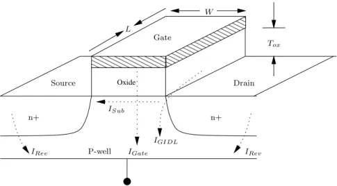
The scaling of VLSI technology has provided the inspiration for many
product evolutions as it gives a scaling of the transistor dimensions, as
illustrated in Figure 2.8, where the length and the width are scaled by a
factor of k. That means the new dimensions are given by L = L k , L = L k
and T ox = T k
ox. This will result in a transistor area reduction up to k 1
2and also increase the transistor speed. Moreover, an expected decrease
in transistor power dissipation as known as currents should be equally
reduced.
00000 00000 00000 11111 11111 11111
0000000 0000000 0000000 0000000 0000000 0000000 0000000
1111111 1111111 1111111 1111111 1111111 1111111 1111111
Oxide
W L
n+ n+
Gate
Drain Source
IRev IRev
Tox
P-well ISub
IGIDL
IGate
Figure 2.8: There are four components of leakage sources in NMOS: Subthreshold leakage (I
Sub), Gate-oxide leakage (I
Gate), Reverse biased junction leakage (I
Rev) and Gate Induced Drain Leakage (I
GIDL)
However, when the node size is smaller than 65nm, a formerly ignor- able gate leakage current (I Gate ) keeps raising explosively when the T ox is reduced to T k
oxbecause the depth of gate oxide between first metal layer and P-well is too short. Fortunately, this problem had already been solved by using high-k dielectric materials to replace the conventional silicon based dioxide to improve the gate dielectric. This allows similar device performance, but with a thicker gate insulator, thus avoiding this leakage current. In a similar situation, the Reverse biased Junction (I Rev ) leakage and the Gate Induced Drain Leakage (I GIDL ) can both be suppressed efficiently in the manufacturing process with new materials.
On the other hand, in order to avoid excessively high electric fields in the scaled structure, the input voltage V DD is required to be scaled.
This forces a scaling in the threshold voltage V T , too, otherwise the transistor will not turn off properly. In the past, subthreshold conduc- tion was generally viewed as a parasitic leakage in a state that would ideally have no current. However, now the reduction in V T will result in an increase of subthreshold drain current (I Sub ) with a direction from the drain to the source in a MOSFET. When the transistor is in the subthreshold region or weak-inversion region, it can be defined as [67]:
I Sub = (µC ox V th 2 W
L )e
VGSnVth−VT, (2.4)
where W and L are the dimension of the transistor, µ is a carrier mobil-
2.7 Design Consideration for Iterative Algorithms 23 ity, C ox is the gate capacitance, V th is the thermal voltage kT/q (25mV at a room temperature), V GS is the gate-source voltage, n is a num- ber of the device manufacturing process with a range from 1.0 to 2.5.
These parameters are considered as constant coefficients for subthresh- old leakage problem. Therefore, the major coefficient is the exponent of V GS − V T . Once we decrease the V DD and V T during shrinking the size of the transistor nodes simultaneous, this results in an exponential increase of the subthreshold leakage power dissipation. In early VLSI circuits, I Sub leakage was a small fraction (far less than 5%) of the total power dissipation. However, this expected decrease in power consump- tion now becomes a nightmare when the node size is smaller than 65nm (could be more than 50%). So far, the most efficient way to reduce the I Sub leakage power is power gating, when the entire macro is turned off.
2.7 Design Consideration for Iterative Algorithms
With aforementioned design issues, we have to consider the relationship between iterative algorithms and design criteria for circuit implemen- tation. First of all, as mentioned in Section 2.4, we already know that the system level stage provides the most opportunities to reduce the power dissipation. On the other hand, according to the source of power dissipation in Section 2.6, the major sources of power dissipation are dynamic and leakage power dissipations in CMOS circuit. Therefore, to design a low power iterative architecture that can reduce both dy- namic and static power dissipations significantly at the system level is one of the major topics in this thesis. In the following chapters, a VLSI design concept will be clarified by four different iterative algorithm- s/methodologies. These hardware solutions not only balance with the circuit design criteria (area, timing and power) but also retain the good quality of results.
Iterative algorithms usually have a common character, more precise
computation or approximation per iteration step will result in more
area overhead for iterative hardware core. On the one hand, less pre-
cise iteration steps will cause slower convergence property. On the other
hand, more precise iteration steps will consume more energy. Here we
will elaborate two iterative examples, CORDIC based QDCIT trans- formation for video compression and parallel Jacobi method for EVD.
They will be handled carefully with a balance between the cost/area, convergency/timing and energy/power.
On–chip network emerges for the next generation SoC and becomes more and more important. With the need for supporting many mul- timedia standards in a single chip, it has been predicted more than one thousand processor units will be integrated together in the future.
However, current bus methodology is facing a critical challenge of data switching for supporting large scale SoC, especially when these proces- sor units are heterogeneous. Moreover, the timing closure will become extremely difficult to be obtained. Therefore, the choice between the ordinary bus-based system and switching based network is a critical design issue especially when the data transfers are irregular. Later, we will show how to utilize this switching feature for Sparse Matrix-Vector Multiplication (SMVM) when solving systems of linear equations iter- atively.
2.8 Summary
In this chapter, a brief introduction to the concerns of today’s nanoscale VLSI design concepts was given. It was shown that dealing with the power dissipation problem became one of the important tasks concern- ing an ASIC development. It will cause very huge efforts for both verifi- cation and implementation when the power sources are not guaranteed.
Therefore, design engineers must carefully think about the relationship between the design criteria (area, timing and power/energy) and the proper way how to realize iterative algorithms in hardware. In next chapter, we will start to discuss the relationship between these im- portant design issues by a well–known iterative algorithm, “CORDIC”
algorithm, which can be used to accelerate many digital functions and
applications in signal processing.
3 CORDIC Algorithm
COordinate Rotation DIgital Computer (CORDIC) is a typical itera- tive algorithm which is used to accelerate many digital functions and applications in signal processing. In this chapter, a brief introduction to the generic definition of the CORDIC algorithm with orthogonal ro- tation mode will be given first in Section 3.1. Then the extension of CORDIC to linear and hyperbolic modes will be further explained in Section 3.2. In Section 3.3, three different dependence flow graphs for the CORDIC hardware implementation will be described and compared in Section 3.4.
3.1 Generic CORDIC Algorithm
Digital Signal Processing (DSP) algorithms exhibit an increasing need for the efficient implementation of complex arithmetic operations. The computation of trigonometric functions, coordinate transformations or rotations of complex valued phases are almost naturally involved with modern DSP algorithms. Popular application examples are algorithms used in digital communication technology and in adaptive signal pro- cessing. There are many applications using the CORDIC algorithm, such as solving systems of linear equations [2, 4, 55, 60], computation of eigenvalues and singular values [30,38,102], Discrete Wavelet Transform (DWT) [28,103], Discrete Cosine Transform (DCT) [75,112] and digital filters [31, 32, 115]. The CORDIC algorithm offers the opportunity to calculate all the desired functions and applications in a rather simple and elegant way in circuit design [6].
The CORDIC algorithm was first presented by Jack Volder in 1959
[122] for the computation of trigonometric function, multiplication, divi-
sion, data type conversion, and later generalized to hyperbolic function
Table 3.1: Three different rotation types of CORDIC with both rotation and vector modes used for implementing the digital processing algorithms (said n iterations and rotated with a target angle φ
t)
Mode Operation
Orthogonal x n = x 0 cos φ t − y 0 sin φ t
Rotation y n = y 0 cos φ t + x 0 sin φ t
z n = 0 Orthogonal x n = p
x 2 0 + y 2 0 Vector y n = 0
z n = arctan(y 0 /x 0 ) = tan − 1 (y 0 /x 0 ) Linear x n = x 0
Rotation y n = y 0 + x 0 · z 0
z n = 0 Linear x n = x 0
Vector y n = 0
z n = z 0 − y 0 /x 0
Hyperbolic x n = x 0 cosh φ t − y 0 sinh φ t
Rotation y n = y 0 cosh φ t + x 0 sinh φ t
z n = 0 Hyperbolic x n = p
x 2 0 − y 0 2 Vector y n = 0
z n = arctanh(y 0 /x 0 ) = tanh − 1 (y 0 /x 0 )
by Walther [124]. A large variety of operations can be easily realized by the structure of CORDIC algorithm [50,56,83]. There are three primary types of CORDIC algorithm, the orthogonal, the linear and the hyper- bolic. Each type has two basic operation modes, rotation and vector, which are summarized in Table 3.1. The CORDIC algorithm can be realized as an iterative sequence of add, sub and shift operations. Due to the simplicity of the involved operations, the CORDIC algorithm is very well suited for VLSI implementation.
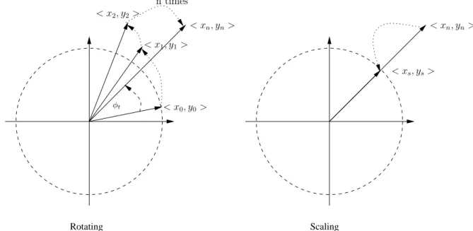
A CORDIC algorithm provides an iterative method of performing
vector rotations. The general form of the orthogonal rotation CORDIC
3.1 Generic CORDIC Algorithm 27 mode is defined as:
x ′ = x cos φ t − y sin φ t
y ′ = y cos φ t + x sin φ t , (3.1) which rotates the input vector < x, y > in the Cartesian coordinate system by a rotation angle φ t . Then this equation can be rearranged as: x ′ = cos φ t (x − y tan φ t )
y ′ = cos φ t (y + x tan φ t ). (3.2) To further simplify it, we can restrict the rotation angle tan φ t to tan φ t = ± 2 − i , such that the multiply operation by the tangent part is reduced to shift operations. This alters Equation 3.2 to become a sequence of arbitrary elementary rotations. Since the decision at each iteration i is fixed, the cos2 − i = cos2 i becomes a constant number. The new iterative rotation can now be defined as:
x i+1 = K i (x i − y i · d i · 2 − i ) y i+1 = K i (y i + x i · d i · 2 − i )
K i = cos(tan − 1 2 − i ) = √ 1+2 1
−2id i = ± 1
i = 0, 1, 2, 3, . . . n.
(3.3)
Removing the scaling factor K i from the iterative part yields a sim- ple shift-add algorithm for orthogonal rotation CORDIC. After several iterations, the product of K i factors will converge to a constant coef- ficient 0.607252. The exact gain depends on the number of iterations:
A n = Q
n
√ 1 + 2 − 2i ≈ 1.646762 = K 1
n
. In the mode of orthogonal rota- tion, the angle accumulator is added to the Equation 3.4.
x i+1 = x i − y i · d i · 2 − i y i+1 = y i + x i · d i · 2 − i z i+1 = z i − d i · tan − 1 2 − i
d i = − 1 when z i < 0 else + 1.
(3.4)
The angle accumulator is initialized with the input rotation angle.
The rotation direction at each iteration i is decided by the magnitude
of the residual angle in the angle accumulator. If the residual angle is
Scaling Rotating
< x
n, y
n>
< x
s, y
s>
< x
0, y
0>
< x
n, y
n>
< x
2, y
2>
< x
1, y
1>
n times
φt
Figure 3.1: CORDIC rotating and scaling a input vector < x
0, y
0> in the orthogonal rotation mode
positive, then the d i is set to +1 otherwise -1. After serveral iterations, it will produce the following results:
x n = A n (x − y tan z 0 ) y n = A n (y + x tan z 0 ) z n = 0.
(3.5)
In Figure 3.1, an example for the generic CORDIC processor rotating an input vector < x 0 , y 0 > with a target rotation angle φ t is shown. The CORDIC processor rotates it by the desired rotation angle iteratively, said n times (usually n = 32 with the single floating precision). After that, a constant scaling value K = 0.607252 will be applied to the rotated vector < x n , y n > in order to scale the rotation results.
Moreover, for the orthogonal vector mode, the CORDIC rotates the input vector through whatever angle is necessary to align the resulting vector with the x axis. That means the direction d i is dependent on the current y i instead of z i . Equation 3.4 can be modified as:
x i+1 = x i − y i · d i · 2 − i y i+1 = y i + x i · d i · 2 − i z i+1 = z i − d i · tan − 1 2 − i
d i = − 1 when y i ≥ 0 else + 1.
(3.6)
3.1 Generic CORDIC Algorithm 29
Rotating
n times
< x
n, y
n>
< x
0, y
0>
< x
1, y
1>
< x
2, y
2>
φn
![Figure 2.3: Relative delays of interconnection wire and gate in nanoscale level (regen- (regen-erated figure from International Technology Roadmap for Semiconductors 2003) [57]](https://thumb-eu.123doks.com/thumbv2/1library_info/3668534.1504169/30.892.198.689.142.488/figure-relative-interconnection-nanoscale-international-technology-roadmap-semiconductors.webp)
![Figure 4.5: Flow graph of an 8–point FDCIT Transform with five configurable modules for multiplierless DCT and integer transforms [106]](https://thumb-eu.123doks.com/thumbv2/1library_info/3668534.1504169/63.892.137.752.133.509/figure-fdcit-transform-configurable-modules-multiplierless-integer-transforms.webp)