www.small-journal.com
Linearly Polarized Electroluminescence from MoS 2
Monolayers Deposited on Metal Nanoparticles: Toward Tunable Room-Temperature Single-Photon Sources
Robin P. Puchert, Felix J. Hofmann, Hermann S. Angerer, Jan Vogelsang, Sebastian Bange, and John M. Lupton*
R. P. Puchert, Dr. F. J. Hofmann, H. S. Angerer, Dr. J. Vogelsang, Dr. S. Bange, Prof. J. M. Lupton
Institut für Experimentelle und Angewandte Physik Universität Regensburg
93053 Regensburg, Germany E-mail: john.lupton@ur.de
The ORCID identification number(s) for the author(s) of this article can be found under https://doi.org/10.1002/smll.202006425.
DOI: 10.1002/smll.202006425
1. Introduction
Transition-metal dichalcogenide (TMDC) monolayers hold potential for future optoelectronic devices[1–3] due to their Break junctions in noble-metal films can exhibit electroluminescence (EL) through inelastic electron tunneling. The EL spectrum can be tuned by depositing a single-layer crystal of a transition-metal dichalcogenide (TMDC) on top. Whereas the emission from the gaps between silver or gold nanoparticles formed in the break junction is spectrally broad, the hybrid metal/TMDC structure shows distinct luminescence from the TMDC material. The EL from individual hotspots is found to be linearly polarized, with a polarization axis apparently oriented randomly. Surprisingly, the degree of polarization is retained in the EL from the TMDC monolayer at room temperature. In analogy to polarized photoluminescence experiments, such polarized EL can be interpreted as a signature of valley-selective transitions, suggesting that spin-flip transitions and dephasing for excitons in the K valleys are of limited importance. However, polarized EL may also originate from the metal nanoparticles formed under electromigration which constitute optical antenna structures. Such antennae can apparently change over time since jumps in the polarization are observed in bare silver-nanoparticle films.
Remarkably, photon-correlation spectroscopy reveals that gold-nanoparticle films exhibit signatures of deterministic single-photon emission in the EL, suggesting a route to designing room-temperature polarized single-photon sources with tunable photon energy through the choice of TMDC overlayer.
unusual direct bandgap at non-zero momentum in k-space,[4–8] resulting in unique optical dipole-selection rules.
These give rise to the valley degree of freedom,[2,9] which enables individual exci- tons to exist simultaneously at two distinct points in k-space, K and K′. This excitonic valley degree of freedom manifests itself in valley-selective, that is, polarized, exci- tation characteristics, and can give rise to linearly polarized luminescence provided that valley coherence is preserved.[4,10]
There is interest in exploiting this addi- tional valley degree of freedom in future devices.[11] While several reports exist on generating electroluminescence (EL) from TMDC monolayers,[12–16] electrically driven emission of linearly polarized light from such 2D crystals at room temperature remains to be demonstrated. In general, the polarized luminescence associated with valley coherence is challenging to observe at room temperature because of swift valley decoherence, which usually occurs on timescales much shorter than the radiative lifetime of the dominant exciton transition in these materials.[6,17–19]
It was recently proposed that plasmonic nanostructures can help to overcome the competing effect of quantum decoher- ence in such systems by lowering the radiative lifetime.[20–22]
Alternatively, the coherence time can be raised, for example, by placing the 2D crystal in an optical cavity, thereby protecting the valley coherence by strong light-matter coupling.[23–25] Also, under conditions of resonance fluorescence of the excitons, that is, where excitons are populated directly in the light cone, the radiative lifetime can become as short as ≈150 fs.[26] In this case, valley coherence effects are expected to become observ- able as linearly polarized fluorescence. While it is known that the valley polarization can be recovered by tuning the excitation energy toward the energy of the excitonic resonance at cryo- genic temperatures,[27,28] a recent report suggested that there may also be valley-coherence effects observable at room tem- perature under resonant optical excitation conditions.[29]
It is challenging to resonantly excite the excitonic transi- tion at room temperature, where transitions are thermally broadened. On the one hand, the degree of resonance with a
© 2021 The Authors. Small published by Wiley-VCH GmbH. This is an open access article under the terms of the Creative Commons Attribu- tion-NonCommercial-NoDerivs License, which permits use and distribu- tion in any medium, provided the original work is properly cited, the use is non-commercial and no modifications or adaptations are made.
narrow-band laser is lowered, on the other hand, the broader the exciton resonance becomes at elevated temperatures, the harder it becomes to filter out the excitation light to probe the fluorescence. We recently introduced a facile approach to study resonance fluorescence in 2D semiconductors by exploiting the intrinsic EL of noble-metal nanoparticle aggregates.[30] This EL is broadband, but can be spectrally focused by resonant cou- pling to the dominant excitonic transition of the TMDC.[31]
The interpretation of the effect is that optical excitation energy, formed in a nanoscale break junction between metallic nano- particles, can be transferred resonantly to the TMDC.[31] Such Förster-type energy transfer becomes possible because, under resonant excitation, the lifetime of the radiative “donor” dipole transition in the nanoparticle hotspot—which relates to the shot noise in the inelastic tunnel junction[32] and the nanopar- ticle plasmon resonances involved—is comparable to that of the
“acceptor” transition in the TMDC monolayer. Here, we there- fore aim to investigate whether signatures of polarization of the EL seen in bare nanoparticle junctions can be preserved in the nanoparticle/TMDC hybrid electroluminescent structures.
2. Results and Discussion
We use EL hotspots from electromigrated thin silver films[33–35]
to excite a monolayer of MoS2. We focus here on MoS2 because this 2D material showed the most pronounced spectral nar- rowing at room temperature, an effect attributed to the par- ticularly strong overlap of the monolayer absorption and the silver-hotspot emission.[31] Due to the electromigration of the silver under current flow, a nanoscale break junction is created in the film[36] and light is generated by inelastic electron tun- neling.[33,36] At the break junction, nanoparticles of different sizes are formed, which constitute a type of plasmonic antenna structure. Such electrically driven plasmonic nanoantennae have been described theoretically[37–39] and realized experimen- tally.[40–42] Nanogap structures have been shown to couple to electronic transitions and therefore offer a variety of applica- tions in optoelectronics and sensing.[43]
Conventional routes to generating EL from 2D materials rely on direct injection of charge carriers into the conduction and valence bands, by incorporating 2D semiconductor materials into quantum-tunneling devices.[44,45] In contrast, we recently demonstrated a different approach in which the electrolumi- nescent hotspots from the electromigrated silver film couple directly to the excitonic transition of TMDC monolayers via resonant energy transfer.[31] Since the binding energy of the exciton is of the order of several hundred meV, such reso- nant pumping of the exciton population occurs at drive biases smaller than those required for direct band-edge electrical injection. As a result, the emission spectrum of the combined metal/2D semiconductor structure is characterized mainly by the narrow excitonic resonance of the monolayer crystal instead of the broadband metal EL.[31]
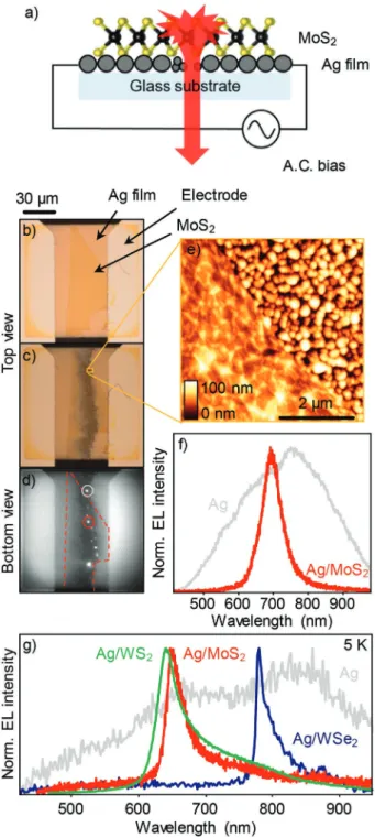
Figure 1a sketches the structure of the silver/MoS2 hetero- structure studied here. We use a thin transparent glass substrate of 100 µm thickness, on which an ≈20 nm thin square silver film of dimensions 100 × 100 µm2 is thermally evaporated. The thin film is contacted by two thicker silver electrodes. After
Figure 1. Electroluminescence (EL) from silver nanoparticles covered with an MoS2 monolayer. a) Sketch of the sample. Light emission is collected through the glass substrate. b) Optical microscope image of a representative sample prior to and c) after electromigration. d) An optical micrograph of the same sample under AC excitation at 100 MHz, illuminated by a white-light LED. The edge of the MoS2 flake is outlined by red dashed lines. e) AFM image of the area marked in panel (c), showing that the flake (left part of the image) overlays the metal-nano- particle surface and remains intact even after electromigration. f) Nor- malized EL spectra of single hotspots of bare silver (grey) and silver/
MoS2 (red) structures. The spectra correspond to the EL spots marked in panel (d). g) Normalized low-temperature EL spectra of single hotspots of bare silver (grey), silver/MoS2 (red), silver/WS2 (green), and silver/
WSe2 (blue) structures.
exfoliation of the MoS2 monolayer using standard procedures, we transfer the 2D crystal directly onto the center of the thin silver layer using the established technique based on the vis- coelasticity of a polydimethylsiloxane (PDMS) substrate.[46] The sample is mounted in a cryostat and kept under vacuum for the duration of the experiment. To electromigrate the thin film, a starting voltage of 1 mV is applied using a source-measure unit, and slowly increased in 1 mV steps until the break junc- tion forms in the silver layer beneath the TMDC monolayer.
The formation of the break junction is witnessed by a sudden increase in the film resistance, that is, a drop in the current at constant voltage, which usually occurs around a bias of 1.2 V. To minimize subsequent electromigration of the break junction, an AC bias is applied to the silver film to drive the EL. Under application of this AC bias, typically at 100 MHz frequency with an amplitude of 1.5–4 V, discrete diffraction-limited spots light up in the plane of the film.[30,31] The light is collected through the glass substrate as described in ref. [31] in detail. Note that the arrangement is such that the silver EL does not pass through the TMDC monolayer. Figure 1b,c shows an example of an optical microscope image of the device before (b) and after electromigration (c), the effect of which is seen by the appear- ance of a narrow gap in the thin silver film. Figure 1d displays the same sample area, recorded in a fluorescence microscope.
The sample is both illuminated by a white LED to be able to identify the pertinent features, and is driven electrically by the AC excitation. Bright discrete, diffraction-limited spots are clearly seen in the image due to the EL. The contours of the MoS2 monolayer are indicated by the red line.
Since electromigration leads to mass transport in the metal film,[47–49] it is instructive to analyze the electromigrated sample with an atomic force microscope (AFM) to determine whether the structure of the TMDC monolayer is preserved. Figure 1e shows a non-contact AFM topography image of the break- junction region. The edge of the MoS2 flake is clearly identified as a diagonal running from the top left to the bottom right of the image. Outside of the region of the flake, the silver nano- particle structures formed during electromigration are clearly identified in the AFM image. The flake is discerned from the metal since it appears smoothed out in the topography image.
In effect, the flake spans the nanoparticles rather like the tarp of a tent. Normalized EL spectra recorded from spots with and without TMDC coverage are compared in Figure 1f. The cor- responding spots are marked grey and red in panel (d). The EL spot outside of the overlayer region (grey) is broad and fea- tureless, spanning the entire visible spectrum out into the NIR region. In contrast, the spectrum recorded from the break-junc- tion region with a TMDC overlayer (red) shows a narrow reso- nance characteristic of the MoS2 A-exciton transition.[31] Note that such a rough and disordered metal substrate gives rise to strain in the 2D crystal. This strain ultimately impacts the emis- sion of the TMDC overlayer as we have shown in our previous report, shifting the MoS2 emission to somewhat longer wave- lengths compared to unstrained films.[31] Although the spectral narrowing effect is most prominent for MoS2 at room tempera- ture,[31] we also observe it with other 2D overlayers such as WS2 and WSe2. The effect is particularly dramatic at low tempera- tures. We illustrate this universality in Figure 1g by comparing normalized EL spectra recorded from an individual bare-silver
spot and single spots covered with MoS2 (red), WS2 (green), and WSe2 (blue), all measured on different samples at a nominal temperature of 5 K. Regardless of the material choice, a sharp resonance is discerned, which shows the dominant A-exciton transition of the respective material. In contrast, the bare silver spectrum remains broad even at low temperatures.
Electromigration continues even during AC excitation of the hotpots, although it is much reduced compared to the case of DC excitation. It gives rise to a degree of instability in the hotspot EL as illustrated in the time dependence of the EL spec- trum of a single hotspot in Figure 2a. Over time, the spot emis- sion shows significant blinking and even sudden changes in spectral width, a form of spectral diffusion reminiscent of the spectroscopy of single molecules[50] and quantum dots.[51] The spectrally integrated EL intensity is shown in the lower part of panel (a), revealing that the entire EL almost vanishes intermit- tently. To analyze the degree of polarization of a single EL spot, we have to account for the fluctuations in the EL intensity. These fluctuations prevent us from simply rotating an analyzer in the EL emission pathway. We therefore split horizontal and vertical polarization components of the EL using a Wollaston prism.
Panel (b) illustrates the experimental setup used. The EL beam is passed through a rotating half-wave plate to define a plane of polarization, and is subsequently split into two orthogonally polarized components, horizontal (H) and vertical (V). The two components are recorded on separate chip areas of the camera.
Figure 2c illustrates the analysis procedure. By normalizing the vertically polarized intensity component, the effect of blinking is mitigated so that the intensity time trace can be fitted by a cosine-squared function following Malus’ law. From such a fit (red line) the effective modulation depth M = (Imax − Imin)/
(Imax + Imin) of the EL intensity provides a metric for the degree of polarization of the hotspot EL. Imax and Imin are the maximum and minimum calculated normalized intensities, respectively.
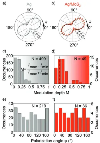
The design of our structure yields approximately ten hot- spots per sample within the break junction. We analyze the polarization characteristics of 499 EL spots from bare silver films and 49 EL spots from silver/MoS2 structures. In the latter case, the involvement of the MoS2 exciton transition in EL is confirmed by inspecting the EL spectrum. Since the exfoliated TMDC monolayers are much smaller than the area of the silver film, there are fewer hotspots beneath the overlayer, and so the overall number of spots sampled here is reduced. It is instruc- tive to graph the polarization anisotropy in polar coordinates, shown in Figure 3a,b for two representative EL spots from bare silver (grey) and the silver/MoS2 structure (red). The normal- ized EL intensity scales from 0 to 1 from the center of the plot toward the outer-most circle of the graph. We define a polari- zation angle ϕ as indicated in the plots, which determines the dominant axis of polarization. Panels (c) and (d) show histo- grams of the modulation depth for silver (c) and silver/MoS2 (d) EL spots. Roughly half of the silver EL spots show a rather weak polarization anisotropy, with a modulation depth of M < 0.2, while ≈40% (200) of the spots exhibit substantial polarization modulation depths with a maximum modulation of M = 0.74.
The devices with the MoS2 overlayer show a similar distribu- tion of M values. This observation is quite remarkable, since the photoluminescence (PL) of MoS2 monolayer crystals at room temperature is generally unpolarized. The most strongly
polarized silver/MoS2 spot shows a modulation depth of M = 0.79, implying a polarization contrast of I
Imax =9 : 1
min
.
Because of the limited signal-to-noise ratio, dipolar radia- tion patterns can be identified conclusively for modulation depths higher than M ≈ 0.15. We therefore chose this value as
a threshold for further analysis of the polarization data, marked by vertical lines in panels (c) and (d). With this cut applied to the data, we can determine meaningful values for the polariza- tion angle ϕ. The corresponding histograms of the distribution of these values are shown in panels (e,f). Evidently, there is no preferential direction of polarization in either case. During elec- tromigration, nanoparticles tend to form in a line orthogonal to the direction of current flow in the film, as seen in Figure 1c.
Intuitively, one may therefore have expected to observe some preference in emission dipole orientation with respect to the ori- entation of the tunnel junctions. This does not appear to be the case. Since each spot has different polarization characteristics, on average, the EL of an ensemble of spots appears unpolarized.
The question now arises as to why the MoS2 EL can acquire such a high degree of polarization. This behavior could be expected, since the excitonic valley coherence, and therefore the PL polarization under resonant excitation, essentially fol- lows the excitation polarization.[4] However, there are two effects responsible for the linear polarization of the EL. The first is that a nanoscale break junction in a noble metal film effectively constitutes an optical antenna,[37–43] which is known Figure 2. Measuring the polarization of a blinking EL hotspot. a) 2D
color-coded plot showing the blinking behavior and spectral diffusion of a single spot with time. The spectrally-integrated intensity is plotted below. b) Experimental setup used to remove the effect of blinking in determining the polarization anisotropy. The EL beam is guided through a half-wave plate and a Wollaston prism, splitting it up into vertically polarized and horizontally polarized components which are detected separately on an imaging camera. c) The half-wave plate is rotated by an angle α and the normalized intensity is determined for each angle (blue circles). Subsequently, the intensity trace is fitted by a cosine-squared function (red) according to Malus’ law.
Figure 3. Polarized EL from single hotspots. a,b) Polar plots of the EL from a single hotspot in bare silver (grey) and silver/MoS2 structures (red). Circles mark the data, which is fitted by a cosine-squared depend- ency. c,d) Histograms of the modulation depth M. A minimum threshold is set at M > 0.15 (vertical dashed black line) to extract the e,f) phase- angle distribution of the polarization.
to influence the polarization of light emission from 2D semi- conductor crystals under optical excitation.[52] The second effect is that, under the resonant excitation of the neutral A-exciton in the MoS2 monolayer by non-radiative Förster-type fluorescence resonance energy transfer,[31] the radiative lifetime can become as short as 150 fs since it is primarily bright exci- tons that are excited resonantly within the light cone.[26] Under these conditions, radiative decay can compete with the sub- picosecond valley decoherence of TMDC monolayers.[17–19] The degree of linear polarization in emission, the linear dichroism
P P τ
= +τ
/ 1
linear 0 A
coherence
,[4,10,53] relates to the magnitude of the initially induced valley coherence P0,[10] the A-exciton lifetime τA, and the valley coherence time τcoherence. Reduction of the neutral A-exciton lifetime τA through resonant coupling to the emissive dipole formed in the silver-nanoparticle hotspot maximizes Plinear. This process is quite distinct from previous approaches based merely on enhancing the radiative rate of the A-exciton, that is, on lowering τA, to generate signatures of valley coherence in PL under resonant optical excitation.[20,54,55]
From the blinking behavior, shown in Figure 2a, one could conceivably also expect sudden changes in the polarization char- acteristics provided that the blinking arises due to continued electromigration of the hotspot, which changes its morphology.
While all of the spots discussed in the analysis of Figure 3 were stable during the measurement and did not show changes in the modulation depth with time, it is indeed possible to iden- tify single EL spots in bare silver films which change their polarization state over time. Figure 4 shows the evolution of the polarization anisotropy of such a spot. Panel (a) plots the nor- malized vertical polarization component of the EL intensity as a function of time. In this example, we identify four different polarization states which arise from this single spot over the duration of the measurement, marked A-D in red, blue, yellow, and green. The hotspot intensity is plotted in the lower part of panel (a). While the change in polarization phase angle in the transition from region C to D coincides with a sudden change in intensity, this feature is not universal. The phase jumps in the polarization and the changes in modulation depth are best visualized in the polar plots in panel (b). The hotspot does not appear to move in the microscope image over the course of the measurement. Since light emission is caused by inelastic electron tunneling in the nanoparticle gap, the dipolar polariza- tion pattern in the far field reflects the underlying nanoparticle geometry and therefore the effective orientation of the nanopar- ticle optical antenna. We propose that the ongoing electromi- gration during electrical excitation leads to different tunneling channels forming between nanoparticles. These channels open up and close down again in the course of the measurement, resulting in EL emerging from tunnel contacts of different ori- entation in the plane and therefore with different degrees of polarization and different polarization directions.
Finally, we turn to a particularly interesting aspect relating to EL from noble-metal nanoparticle structures: the possibility of electrically driven deterministic single-photon emission at room temperature.[56] Combined with our demonstration of the tuna- bility of the EL spectrum through the choice of the TMDC over- layer,[31] and the apparent polarization of the EL, single-photon emission could be of interest for quantum-communication
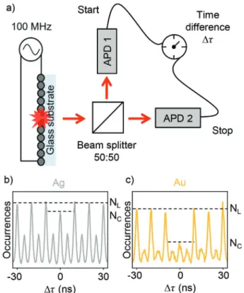
applications. Nanoparticle break junctions with and without TMDC overlayers can be fabricated equally well with silver and gold films. To probe the degree of non-classical photon emis- sion, we analyze the EL photon statistics using two avalanche photodiodes (APDs) in a Hanbury Brown Twiss configuration as shown in the cartoon in Figure 5a. The EL beam passes through a beam splitter and the photon coincidence rate on the two photodetectors is computed. In the second-order cross cor- relation function of the EL intensity, plotted in Figure 5b as a Figure 4. Jumps in the polarization plane of the EL of a single bare-silver hotspot. a) Normalized and absolute intensity of a selected bare-silver EL spot versus the rotation angle α of the half-wave plate. Over the duration of the experiment, for a rotation of the half-wave plate by 1800°, four dif- ferent polarization states A–D (red, blue, yellow, green) are identified. b) Polar plots of the polarization anisotropy of the EL intensity of the color- coded areas in (a). The EL spot changes its polarization state from linearly polarized (A) to unpolarized (B) and back again (C, D). These changes coincide with a jump in polarization phase angle ϕ as defined in Figure 3a.
function of the delay time Δτ between detection events on the two APDs, distinct peaks reflect the 100 MHz AC excitation fre- quency of the nanoparticles. Every 10 ns a large peak appears with a smaller peak at 5 ns delay time in between arising from the reversal of the bias.[57] To probe the degree of non-classical photon emission, we examine the ratio of the height of the cen- tral peak at time delay Δτ = 0, NC, over the lateral-peak height NL at delay times Δτ ≠ 0. EL from electromigrated silver films clearly shows non-classical sub-Poissonian photon statistics, with NC/NL = 0.88, although the effect is quite weak. In con- trast, for gold nanoparticles, fabricated by the same electromi- gration procedure, NC/NL = 0.42, suggesting that, on average, fewer than two photons are emitted at a time. While the struc- ture is not a perfect single-photon source, that is, it does not show perfect photon antibunching, it is remarkable to achieve such a high degree of non-classical photon emission in a mac- roscopic structure, at room temperature.
A possible explanation for the large difference between the two metals, gold and silver, may be linked to the difference in radiative lifetimes of the emissive transitions.[56] Unfortunately, the luminescence lifetime cannot be resolved for two reasons.
First, the time resolution of the APDs is limited to ≈300 ps.
Second, under electrical excitation as used here, the rate at which photons can be emitted is limited by the time it takes
to charge the nanoparticle gap. This time is the equivalent of the “RC” time in a conventional electrical circuit consisting of a capacitor and a resistor. Using photon correlation spectroscopy, we previously estimated this time to be of order 2 ns,[31] which is likely much longer than the luminescence lifetimes of either of the nanoparticle structures. We also note that the micro- scopic origin of this pronounced photon antibunching is still not entirely clear. Gonzalez et al. suggested that this discrete emission arises due to the formation of molecule-like atomic clusters of gold atoms within the break junction,[56] which can support well-defined electronic transitions in analogy to photon antibunching from single dye molecules or quantum dots.
However, the model invoked to explain EL from metal tips in scanning tunneling microscopy involves the shot noise in single-electron tunnelling,[32] which could conceivably also give rise to photon antibunching. The topic therefore remains of interest for future research.
It would of course be appealing to demonstrate such non- classical photon emission in EL with the structures comprising TMDC overlayers. However, thus far, we have not been able to identify such photon correlations in gold/MoS2 devices con- clusively mainly for the reason that the gold EL spectrum is of lower energy and, in parts, spectrally narrower than that of silver, making it challenging to discern conclusively from the A-exciton transition of the overlayer. While the obvious goal would be to achieve deterministic single-photon emission at room temperature, cooling the device as illustrated in Figure 1g should facilitate discrimination between gold and TMDC EL, although detecting photon correlations at low temperatures rather than merely measuring EL spectra will require substan- tial modifications to the setup.
3. Conclusion
We have introduced a device structure which exhibits partially lin- early polarized EL from the excitonic transition of MoS2 overlayers deposited on noble-metal nanoparticles. The structure relies on resonant coupling between dipoles formed in the electrolumines- cent hotspots of the metal nanoparticles and the excitonic reso- nance in the 2D crystal monolayer. Such devices could conceivably find future application in optical on-chip communication[58]
and point to a new direction for the integration of “valleytronic”
devices[59] using 2D TMDC semiconductors combined with defined plasmonic nanostructures. However, we note that, at pre- sent, it is not possible to conclusively decide whether the remark- able degree of polarization in the EL of the TMDC overlayer is indeed a signature of the preservation of valley coherence due to the resonant excitation, or whether it is simply a consequence of the nanoparticle arrangement, which acts as an effective optical antenna to couple the hotspot EL to the optical far field.[39] The fact that the distribution of the modulation depth values is similar for hotspots with and without the overlayer suggests that there is no additional depolarization effect present in the TMDC EL, and that it is therefore indeed the latter antenna effect rather than the valley coherence which determines the polarization effect. To con- clusively probe the contribution of valley coherence to the linearly polarized luminescence will require measurements of the EL as a function of temperature and magnetic field.[5]
Figure 5. Signatures of single-photon emission. a) The photon statistics of an individual diffraction-limited EL hotspot is analyzed by means of a Hanbury Brown Twiss intensity-correlation setup, where the EL is passed through a beam splitter and the photon coincidence rate on two photo- detectors is computed. b) The EL from silver-nanoparticle structures shows non-classical photon statistics but no clear signature of single- photon emission, whereas the c) EL from hotspots in gold-nanoparticle films implies emission of significantly fewer than two photons at once, approaching the limit of photon antibunching.
4. Experimental Section
Sample Preparation: The devices were designed using a two-step photolithographic process to ensure reproducible break-junction formation. In a first step, square regions of 100 × 100 µm² were defined with a mask aligner in a spin-coated double photoresist layer (AR300- 80, AR-P5350, Allresist) on a 100 µm glass substrate, and subsequently developed (AR300-35, Allresist). After evaporation of a 20 nm thick silver or gold film, the active structure was formed by lift-off of the residual photoresist in an acetone bath. In a second step, silver or gold electrodes of 150 nm thickness were defined. The homogeneity of the process ensured that the break junction formation always occurred in the center of the thin silver film. Nominally undoped TMDC bulk crystals with high purity (>99.995%) were purchased from the HQ Graphene.
TMDC monolayers were mechanically exfoliated from the bulk crystals under ambient conditions onto a PDMS film and subsequently stamped onto the silver or gold film by a deterministic dry transfer based on the viscoelasticity of the PDMS film.[46] With this method, it was possible to control the position of the flake on the metal film with micrometer precision. It should be noted that there may be some contamination of the surface of the TMDC due to the conventional ambient transfer method, for example due to the formation of a thin layer of water, but this clearly did not impair the device operation since intrinsic excitonic resonances were evidently resolved in EL. Preparation under inert-gas conditions in a glovebox could conceivably narrow the excitonic resonances further.
Optical Spectroscopy: Electromigration was carried out under vacuum (10−6 mbar) and at room temperature. The sample was mounted in a cryostat (Supertran ST-500, Janis Research) and connected to a source-measure unit (Keithley 2401). For electrical excitation, the electromigrated sample was connected to an amplified high-frequency source (amplifier ZHL-2-S, Mini Circuits; HF generator 83732A, Agilent Technologies). The frequency was set to 100 MHz and the voltage was set to 1.5–4 V, optimized for hotspot brightness and stability. EL was collected by a microscope objective (SLCPlanFl 40 ×, Olympus) through the glass substrate. Images of the sample, illuminated by an external white LED, were recorded with an sCMOS camera (Orca-Flash 4.0, Hamamatsu), and the spectra were measured with a spectrometer and a charge-coupled device camera (Pixis, Princeton Instruments). The low-temperature EL spectra in Figure 1g were acquired by cooling the device down to liquid-helium temperature in the cryostat and keeping the temperature constant by an automated heating element mounted on the cold finger.
Polarization Measurements: To determine the modulation depth M, the EL was collected by a microscope objective and subsequently passed through a half-wave plate (AHWP05M-600/400–800 nm, Thorlabs), followed by a Wollaston prism (WPM10, Thorlabs), which split up the emission into a vertically and horizontally polarized part. The half-wave plate was rotated in 5°-steps and for every angle a widefield image of the EL was taken. The intensity of individual spots was determined for each angle by summing up the intensity of every pixel in a symmetric region around the diffraction-limited spot projected onto the sCMOS- camera, and by normalizing one of the polarization channels according
to I I
I I
= +
norm v
v h. From the normalized intensity Inorm the modulation depth was calculated as described in the main text.
Photon Correlation Measurements: The photon correlation measurements were performed using an oil-immersion objective (UPLSAPO × 60, 1.35 numerical aperture, Olympus), where the light was detected by two single-photon detectors (PicoQuant SPAD 20) in an Hanbury Brown Twiss arrangement with a 50:50 beam splitter (Thorlabs BS013) between both detectors. The photon correlation data were analyzed using a commercial software package (PicoQuant SymPhoTime 64).
AFM Measurement: The AFM topography image was taken with silicon probes (Nanosensors SSS-NCHR) using a Park Systems XE-100 operating in “non-contact” amplitude-modulation mode under ambient conditions in a vibration-isolated acoustic enclosure.
Acknowledgements
Financial support is gratefully acknowledged from the Deutsche Forschungsgemeinschaft (DFG, German Research Foundation)—
Project-ID 314695032—SFB 1277 project B03.
Open access funding enabled and organized by Projekt DEAL.
Conflict of Interest
The authors declare no conflict of interest.
Keywords
electroluminescence, optoelectronics, plasmonics, single-photon emission, van der Waals crystals
Received: October 14, 2020 Revised: December 3, 2020 Published online:
[1] K. S. Novoselov, D. Jiang, F. Schedin, T. J. Booth, V. V. Khotkevich, S. V. Morozov, A. K. Geim, Proc. Natl. Acad. Sci. USA 2005, 102, 10451.
[2] G. Wang, A. Chernikov, M. M. Glazov, T. F. Heinz, X. Marie, T. Amand, B. Urbaszek, Rev. Mod. Phys. 2018, 90, 021001.
[3] P. Merkl, F. Mooshammer, S. Brem, A. Girnghuber, K.-Q. Lin, L. Weigl, M. Liebich, C.-K. Yong, R. Gillen, J. Maultzsch, J. M. Lupton, E. Malic, R. Huber, Nat. Commun. 2020, 11, 2167.
[4] A. M. Jones, H. Yu, N. J. Ghimire, S. Wu, G. Aivazian, J. S. Ross, B. Zhao, J. Yan, D. G. Mandrus, D. Xiao, W. Yao, X. Xu, Nat. Nanotechnol. 2013, 8, 634.
[5] G. Wang, X. Marie, B. L. Liu, T. Amand, C. Robert, F. Cadiz, P. Renucci, B. Urbaszek, Phys. Rev. Lett. 2016, 117, 187401.
[6] K. Hao, G. Moody, F. Wu, C. K. Dass, L. Xu, C.-H. Chen, L. Sun, M.-Y. Li, L.-J. Li, A. H. MacDonald, X. Li, Nat. Phys. 2016, 12, 677.
[7] K. F. Mak, C. Lee, J. Hone, J. Shan, T. F. Heinz, Phys. Rev. Lett. 2010, 105, 136805.
[8] A. Splendiani, L. Sun, Y. Zhang, T. Li, J. Kim, C. Y. Chim, G. Galli, F. Wang, Nano Lett. 2010, 10, 1271.
[9] K. F. Mak, D. Xiao, J. Shan, Nat. Photonics 2018, 12, 451.
[10] D. H. Kim, M. J. Shin, D. Lim, J. Korean Phys. Soc. 2015, 66, 806.
[11] J. Xiao, M. Zhao, Y. Wang, X. Zhang, Nanophotonics 2017, 6, 1309.
[12] R. S. Sundaram, M. Engel, A. Lombardo, R. Krupke, A. C. Ferrari, P. Avouris, M. Steiner, Nano Lett. 2013, 13, 1416.
[13] Y. Ye, J. Xiao, H. Wang, Z. Ye, H. Zhu, M. Zhao, Y. Wang, J. Zhao, X. Yin, X. Zhang, Nat. Nanotechnol. 2016, 11, 598.
[14] D.-H. Lien, M. Amani, S. B. Desai, G. H. Ahn, K. Han, J.-H. He, J. W. Ager, M. C. Wu, A. Javey, Nat. Commun. 2018, 9, 1229.
[15] J. Wang, I. Verzhbitskiy, G. Eda, Adv. Mater. 2018, 30, 1802687.
[16] M. Paur, A. J. Molina-Mendoza, R. Bratschitsch, K. Watanabe, T. Taniguchi, T. Mueller, Nat. Commun. 2019, 10, 1709.
[17] M. M. Glazov, T. Amand, X. Marie, D. Lagarde, L. Bouet, B. Urbaszek, Phys. Rev. B 2014, 89, 201302.
[18] M. M. Glazov, E. L. Ivchenko, G. Wang, T. Amand, X. Marie, B. Urbaszek, B. L. Liu, Phys. Status Solidi B 2015, 252, 2349.
[19] M. Selig, G. Berghäuser, A. Raja, P. Nagler, C. Schüller, T. F. Heinz, T. Korn, A. Chernikov, E. Malic, A. Knorr, Nat. Commun. 2016, 7, 13279.
[20] S. I. Bogdanov, A. Boltasseva, V. M. Shalaev, Science 2019, 364, 532.
[21] T. Chervy, S. Azzini, E. Lorchat, S. Wang, Y. Gorodetski, J. A. Hutchison, S. Berciaud, T. W. Ebbesen, C. Genet, ACS Pho- tonics 2018, 5, 1281.
[22] S. Kim, Y.-C. Lim, R. M. Kim, J. E. Fröch, T. N. Tran, K. T. Nam, I. Aharonovich, Small 2020, 16, 2003005.
[23] Y. J. Chen, J. D. Cain, T. K. Stanev, V. P. Dravid, N. P. Stern, Nat. Photonics 2017, 11, 431.
[24] L. Qiu, C. Chakraborty, S. Dhara, A. N. Vamivakas, Nat. Commun.
2019, 10, 1513.
[25] E. Lorchat, S. Azzini, T. Chervy, T. Taniguchi, K. Watanabe, T. W. Ebbesen, C. Genet, S. Berciaud, ACS Photonics 2018, 5, 5047.
[26] C. Poellmann, P. Steinleitner, U. Leierseder, P. Nagler, G. Plechinger, M. Porer, R. Bratschitsch, C. Schüller, T. Korn, R. Huber, Nat. Mater.
2015, 14, 889.
[27] D. Lagarde, L. Bouet, X. Marie, C. R. Zhu, B. L. Liu, T. Amand, P. H. Tan, B. Urbaszek, Phys. Rev. Lett. 2014, 112, 047401.
[28] G. Kioseoglou, A. T. Hanbicki, M. Currie, A. L. Friedman, B. T. Jonker, Sci. Rep. 2016, 6, 25041.
[29] L. Du, J. Tang, J. Liang, M. Liao, Z. Jia, Q. Zhang, Y. Zhao, R. Yang, D. Shi, L. Gu, J. Xiang, K. Liu, Z. Sun, G. Zhang, Research 2019, 2019, 6494565.
[30] T. H. Lee, J. I. Gonzalez, J. Zheng, R. M. Dickson, Acc. Chem. Res.
2005, 38, 534.
[31] R. P. Puchert, F. Steiner, G. Plechinger, F. J. Hofmann, I. Caspers, J. Kirschner, P. Nagler, A. Chernikov, C. Schüller, T. Korn, J. Vogelsang, S. Bange, J. M. Lupton, Nat. Nanotechnol. 2017, 12, 637.
[32] N. L. Schneider, G. Schull, R. Berndt, Phys. Rev. Lett. 2010, 105, 026601.
[33] J. Lambe, S. L. McCarthy, Phys. Rev. Lett. 1976, 37, 923.
[34] S. L. McCarthy, J. Lambe, Appl. Phys. Lett. 1977, 30, 427.
[35] B. Laks, D. L. Mills, Phys. Rev. B 1979, 20, 4962.
[36] D. Hone, B. Mühlschlegel, D. J. Scalapino, Appl. Phys. Lett. 1978, 33, 203.
[37] J. C. Prangsma, J. Kern, A. G. Knapp, S. Grossmann, M. Emmerling, M. Kamp, B. Hecht, Nano Lett. 2012, 12, 3915.
[38] M. Parzefall, L. Novotny, ACS Photonics 2018, 5, 4195.
[39] M. Parzefall, L. Novotny, Rep. Prog. Phys. 2019, 82, 112401.
[40] J. Kern, R. Kullock, J. Prangsma, M. Emmerling, M. Kamp, B. Hecht, Nat. Photonics 2015, 9, 582.
[41] C. Zhang, J.-P. Hugonin, A.-L. Coutrot, C. Sauvan, F. Marquier, J.-J. Greffet, Nat. Commun. 2019, 10, 4949.
[42] J. Qin, Y. Liu, H. Luo, Z. Jiang, W. Cai, L. Wang, ACS Photonics 2019, 6, 2392.
[43] J. J. Baumberg, J. Aizpurua, M. H. Mikkelsen, D. R. Smith, Nat.
Mater. 2019, 18, 668.
[44] M. Parzefall, P. Bharadwaj, A. Jain, T. Taniguchi, K. Watanabe, L. Novotny, Nat. Nanotechnol. 2015, 10, 1058.
[45] M. Parzefall, Á. Szabó, T. Taniguchi, K. Watanabe, M. Luisier, L. Novotny, Nat. Commun. 2019, 10, 292.
[46] A. Castellanos-Gomez, M. Buscema, R. Molenaar, V. Singh, L. Janssen, H. S. J. van der Zant, G. A. Steele, 2D Mater. 2014, 1, 011002.
[47] S. P. Sindermann, A. Latz, G. Dumpich, D. E. Wolf, F. J. Meyer Zu Heringdorf, J. Appl. Phys. 2013, 113, 134505.
[48] S. P. Sindermann, A. Latz, D. Spoddig, C. Schoeppner, D. E. Wolf, G. Dumpich, F. J. Meyer Zu Heringdorf, J. Appl. Phys. 2014, 116, 034502.
[49] R. Hoffmann-Vogel, Appl. Phys. Rev. 2017, 4, 031302.
[50] H. P. Lu, X. S. Xie, Nature 1997, 385, 143.
[51] S. A. Empedocles, R. Neuhauser, K. Shimizu, M. G. Bawendi, Adv. Mater. 1999, 11, 1243.
[52] J. Kern, I. Niehues, P. Tonndorf, R. Schmidt, D. Wigger, R. Schneider, T. Stiehm, S. Michaelis de Vasconcellos, D. E. Reiter, T. Kuhn, R. Bratschitsch, Adv. Mater. 2016, 28, 7101.
[53] K. F. Mak, K. He, J. Shan, T. F. Heinz, Nat. Nanotechnol. 2012, 7, 494.
[54] S. I. Bogdanov, M. Y. Shalaginov, A. S. Lagutchev, C. C. Chiang, D. Shah, A. S. Baburin, I. A. Ryzhikov, I. A. Rodionov, A. V. Kildishev, A. Boltasseva, V. M. Shalaev, Nano Lett. 2018, 18, 4837.
[55] C. Han, J. Ye, Nat. Commun. 2020, 11, 713.
[56] J. I. Gonzalez, T.-H. Lee, M. D. Barnes, Y. Antoku, R. M. Dickson, Phys. Rev. Lett. 2004, 93, 147402.
[57] J. I. Gonzalez, T. Vosch, R. M. Dickson, Phys. Rev. B 2006, 74, 064305.
[58] S. Khasminiskaya, F. Pyatkov, K. Słowik, S. Ferrari, O. Kahl, V. Kovalyuk, P. Rath, A. Vetter, F. Hennrich, M. M. Kappes, G. Gol’tsman, A. Korneev, C. Rockstuhl, R. Krupke, W. H. P. Pernice, Nat. Photonics 2016, 10, 727.
[59] J. R. Schaibley, H. Yu, G. Clark, P. Rivera, J. S. Ross, K. L. Seyler, W. Yao, X. Xu, Nat. Rev. Mater. 2016, 1, 16055.