Fast Triggering in High Energy Physics
Experiments Using Hardware Neural Networks
B. Denby 1 , P. Garda 1 , B. Granado 1 , C. Kiesling 2 , J.-C. Prevotet 1 , A. Wassatsch 2
1 Laboratoire des Instruments et Syst`emes d’Ile de France, Universit´e Pierre et Marie Curie, 4 Place Jussieu, BC 252, F-75252 Paris Cedex 05, France
2 Max-Planck-Institut f¨ur Physik (Werner-Heisenberg-Institut), F¨ohringer Ring 6, D-80805 M¨unchen, Germany
Abstract—High Energy Physics experiments require high-speed triggering systems capable of performing complex pattern recogni- tion at rates of Megahertz to Gigahertz. Neural networks imple- mented in hardware have been the solution of choice for certain experiments. The neural triggering problem is presented here via a detailed look at the H1 level 2 trigger at the HERA accelerator in Hamburg, Germany, followed by a section on the importance of hardware preprocessing for such systems, and finally some new ar- chitectural ideas for using field programmable gate arrays in very high speed neural network triggers at upcoming experiments.
I. I NTRODUCTION
Experimental research in High Energy Physics (HEP) is one area in which the speed advantage of neural networks (NN) im- plemented in parallel hardware has been exploited to great ben- efit. It is interesting to examine such applications in the context of NN research for three reasons:
1) The H1[1] experiment at the HERA accelerator[2] in Ger- many is one of the rare instances of large-scale hardware neural networks playing a pivotal, long-term role in a ma- jor scientific instrumentation system.
2) The incorporation of NN’s into a running experiment that extracts physics results online brings into focus a point under-appreciated in hardware NN design: a realistic hardware NN system must also include hardware prepro- cessing to transform the raw detector data into usable in- put variables.
3) Future HEP accelerators will have even more stringent real-time constraints than existing ones; at the same time, commercial high speed NN hardware is practically non- existent. Some of the new, FPGA-based NN solutions currently proposed by HEP research groups are architec- turally interesting in their own right.
In the following sections, each of these points will be ad- dressed in detail.
A. The HEP Triggering Problem
In experimental HEP, information on the elementary building blocks of matter and the forces between them is extracted from
Corresponding authors: Christian Kiesling cmk@mppmu.mpg.de and Bruce Denby denby@ieee.org and
the debris of collisions of intense, high energy particle beams produced in giant accelerators. The extremely low signal to background ratio for the sought after physics processes - typi- cally 3 to 5 orders of magnitude - presents difficult challenges for the design of data analysis systems of HEP experiments. In experiments at the major accelerator facilities, data produced in building-sized multichannel particle detectors surrounding the interaction regions are accumulated at rates of several Gi- gabytes per second.
As it is not feasible, using today’s technology, to log all of this data onto permanent storage media for later analysis, an online decision-making system is necessary: the experimental trigger. The timing requirements for such a device are rather severe. At the H1 experiment the HERA facility, for example, a new frame of detector data arrives at the trigger system ev- ery 96 nanoseconds, and though pipelining techniques may be used, the latency before full detector readout may not exceed 20 microseconds. The timing constraints at the LHC facility, currently under construction at CERN in Switzerland, will be roughly another order of magnitude more stringent than those at H1.
B. The Case for Neural Networks in HEP
The choice of NN in triggering applications has several mo- tivations.
• In HEP data, discrimination between signal and back- ground is based upon the spatial distribution of particle tracks and energy deposits in the various detector subsys- tems. As the triggering problem is thus essentially one of pattern recognition, it is natural to examine neural network techniques as a possible solution.
• The snapshot-like nature of the HEP datasets - one ‘image’
per particle collision - leads to naturally-time-segmented data sets which lend themselves well to a data-driven ap- proach.
• Finally, the possibility of parallel hardware implementa- tion of neural networks makes them appear a particularly attractive possibility where timing constraints are difficult.
Although the use of hardware NN is by no means the stan-
dard in HEP, certain experiments, including H1, have made very
successful use of them in triggering systems. As a caveat, it
should be pointed out that the networks used in HEP applica- tions are almost exclusively simple MLP’s, albeit rather large ones. It is in the fast hardware implementation of NN trigger systems, and their adaptation to the experimental environment, that research challenges lie, rather than in NN architectures per se.
C. Organization of the Article
In section II, a detailed presentation is given of a neural trig- gering system that has been in successful operation for 5 years - the H1 experiment level 2 trigger[3] at the HERA accelerator in Germany. The system is based upon the CNAPS [4] neural network chip coupled with an FPGA-based preprocessor (the Data Distribution Board or DDB). An overall plan of the ex- periment, the NN architecture, hardware implementation, and a physics result made possible by the NN approach are presented.
Section III expands upon the importance of hardware prepro- cessing for hardware NN applications by presenting an upgrade currently in progress for the H1 preprocessor. The new version, called DDB II, which as its predecessor will be implemented in FPGA’s, will have greatly extended functionality, allowing to perform clustering, matching, ranking, and postprocessing in less than 4 microseconds before passing the final results to the CNAPS trigger boards.
Section IV takes a look at the future of NN implementations for triggering - both for future experiments at HERA and for the even more challenging data taking at the LHC in Switzerland - making note of the fact that commercial hardware capable of servicing these experiments will likely not be available when they begin taking data a few years from now. Two original, highly parallel FPGA designs, one using standard arithmetic and the other digit online (serial) arithmetic, are presented as possible responses to these challenges. In preliminary tests, both permitted to calculate a multilayer perceptron architecture of 128-64-4 in under 1 microsecond, which is already a very encouraging result.
A conclusion is given in section V.
II. T HE H1 E XPERIMENT L EVEL 2 N EURAL N ETWORK
T RIGGER AT HERA A. HERA Accelerator and H1 Experiment
The HERA accelerator [2] is a typical ‘collider’ design. It has a circumference of 6.5 km, accelerating, in separate rings, beams of electrons and protons to very high energy (see the schematic layout of the HERA accelerator complex, including the injector machines in fig. 1). Although the particles in the beams are grouped into discrete packets called ‘bunches’, typ- ically only a single proton and a single electron will enter into collision at each ‘bunch crossing’ (BC). These crossings occur every 96 nanoseconds, and the resulting final state particles are observed in huge detector systems surrounding the point of col- lision.
One of the two detector systems at HERA is the H1-detector [1], which employs a large variety of detection principles (see fig. 2) in the various subdetectors. For the detection of electri- cally charged particles H1 uses an arrangement of ‘wire cham- bers’ or ‘tracking chambers.’ The tracker system is surrounded
Hall North H1
Hall East HERMES
Hall South ZEUS
HERA
Hall West HERA-B
e p
Volkspark Stadion 360m
36 0m R=
79 7m
Tra bre nn ba
hn
Fig. 1. Schematic view of the HERA accelerator complex.
by a calorimeter which measures precisely the direction and en- ergy of charged as well as electrically neutral particles. The calorimeter is enclosed by a superconducting solenoidal mag- net with diameter of about 6 m, allowing to measure the mo- mentum of charged particles via their curvature in the magnetic field. Further details on the H1 detector are given elsewhere [1].
For triggering the apparatus, H1 has installed a scheme of three levels (see fig. 3), two hardware levels and one software level (“level 4”) (an intermediate software level (“level 3”) is foreseen, but not used at present).
In the first level trigger (“level 1”) each of the subdetectors derives a trigger decision based on its data alone. Since the respective trigger processors must be able to make a decision at each bunch crossing, i.e. every 96 ns, the trigger data are shifted through, and processed in, digital pipelines. The length of the pipelines is 24 BC’s and is determined by the memory time of the detector components. Since the execution time for the trigger processors at level 1 is strongly constrained, only coarse subdetector information can be processed. Due to the pipeline technique, on the other hand, the trigger decision at level 1 is deadtime free. The decisions from the various subde- tectors are sent to a central trigger unit, where they can, again due to the limited latency of the trigger level 1, only be sub- jected to logical combinations. The final trigger decision of the first level is delivered after about 2.3 µs (24 BC’s) and the infor- mation prepared and used by the level 1 subdetector processors is transferred to the level 2 system.
At this point the primary deadtime starts; no further triggers
can be accepted until the event buffers are fully read out or a
fast “clear” from the level 2 trigger system has been issued re-
jecting the event. When the event is accepted by the level 2,
the detector readout is initiated and the full event information
is sent to the level 4 processor farm, where an event reconstruc-
tion is performed and the final decision for permanent storage
of the event is taken.
Fig. 2. Schematic view of the H1 detector, showing the various subdetector.
20 µ 2.3 µ s
800 µ s
Tape Output Production
Trigger-levels at H1
s
components
hardwired logic
microprocessor farm microprocessor neural networks
L2 L1
L3
L4
L5
100 ms L2-reject
L1-reject
L3-reject
L4-reject
monitoring on tape
online offline hold-
signal
preselection for physical analysis
Data Selection Tapes dataflow
~5kHz
~200Hz
~50Hz
few Hz 1 B.C.=96ns
(pipelined)
~10MHz
H1 detector
Fig. 3. Schematic view of the H1 trigger scheme.
Fig. 4. The MLP architecture of the neural trigger application, with one input layer, one hidden layer, and one output node. The inherently parallel neural data processing is mapped to a dedicated parallel processor array (see text).
For the level 2 hardware trigger the decision time is limited to 20 µs in order to digest a maximum of 1-2 kHz from level 1 while keeping the deadtime below 2 %. At level 2, the infor- mation from all level 1 processors is available, so that the cor- relations among the various trigger quantities can be exploited.
This is done using a set of hardware NN, as described below.
The output of the level 2 trigger must not exceed 100 Hz which is the maximum rate for the level 4 RISC processor farm. The output rate of level 4 is limited to about 10 Hz.
B. Principles of the H1 Neural Network Trigger
The H1 NN trigger operating in the second trigger level, uti- lizes a standard MLP format (see fig. 4). For the network computations (matrix-vector multiplication and accumulation) a commercial parallel-processor chip is used (the 1064 CNAPS chip by Adaptive Solutions [4], which however is no longer manufactured), while for the preparation of the input quanti- ties and their interfacing to the CNAPS chips, the dedicated hardware preprocessor DDB (described below) has been built.
Due to the high flexibility of programming the CNAPS chip, arbitrary neural algorithms may be realized, provided they fit within the latency of the level 2 (“L2”) trigger of 20 µs. In the L2 Neural Network Trigger of H1 three different algorithms are considered at present:
• Feed Forward Networks: These networks have a fully con- nected three-layer structure with one input layer and one hidden layer (with a maximum of 64 nodes each), and one output node (see fig. 4). A single output node is adequate since the network must only indicate whether the data from the current collision is to be retained or discarded.
The input layer is fed with the components of a vector ~x spanning the “trigger space”, prepared by the preprocess- ing hardware. The value of the output y = F (~x, ~ w) [0, 1]
is used as a discriminator to make the trigger decision.
Network architectures and weights w ~ were optimized of- fline using real and simulated detector data.
• Constructed Nets: For some simple, low-dimensional applications a topological correlator, exploiting the fast matrix-vector multiplication hardware of the CNAPS chip, is used [5]
• Background encapsulators: To avoid possible bias in se-
lecting a specific physics class for training against the
M o n it o ri n g D D B 0 D D B 1 D D B 2 D D B 3 D D B 4 D D B 5 D D B 6 D D B 7 D D B 8 D D B 9 D D B 1 0 D D B 1 1
C N A P S 0 C N A P S 1 C N A P S 2 C N A P S 3 C N A P S 4 C N A P S 5 C N A P S 6 C N A P S 7 C N A P S 8 C N A P S 9 C N A P S 1 0 C N A P S 1 1
V M E S U N / S B u s In te rf ac e
S B u s In te rf ac e
X11 Terminal
Data from Detector To Final Decider
Loading and Control
Fig. 5. Layout of boards in the H1 Neural Network Trigger system. Each network processor (CNAPS) is associated with a preprocessing module (DDB), preparing the net inputs individually for its companion CNAPS board. The system is steered by a VME SPARCstation with remote accessibility.
background, a self-organizing network for encapsulating the background is under study.
The present strategy of using the networks is as follows. Each of the networks is trained for a specific physics channel and is coupled to a set of level 1 subtriggers particularly efficient for that channel. Because the level 1 subtriggers are sufficiently relaxed to be efficient, their rate is in many cases unacceptably high. The level 2 trigger therefore has the task to reduce the excess background rate in the subtrigger set while keeping the efficiency for the chosen physics channel high.
Detailed investigations have shown that small networks trained for specif ic physics reactions, working all in parallel, are more efficient than a single larger net trained on all physics reactions simultaneously. More importantly, when putting these nets into a real trigger application, this degree of modularity is extremely helpful when additional triggers for new kinds of physics reactions are to be implemented: there is no need to re- train the other nets, the new physics net is simply added to the group of the others.
At present, 12 networks are running in parallel, mostly opti- mized for production of particles called ‘vector mesons’, which are difficult to separate from the background at level 1. Typical rate reductions are between a factor of 5 to over a hundred.
C. L2 Trigger Hardware
According to the principles described above, the hardware realization for the network trigger is chosen as follows (see fig. 5). Receiver cards collect the incoming L1 trigger informa- tion of the various subdetectors and distribute them via a 128
bit wide L2 bus to the DDB units. Each DDB is able to pick up a programmable set of items from the L2 data stream. It performs some basic operations on the items (e.g bit summing) and provides an input vector of maximally 64 8bit words for one CNAPS/VME board. Controlling and configuring of the complete system is done by a THEMIS VME SPARCstation, which is located in the CNAPS crate.
1) The CNAPS board: The algorithms calculating the trig- ger decision are implemented on a VME board housing the CNAPS chip. This chip is an array of parallel fixed-point arith- metic processors in SIMD architecture. The CNAPS-1064 chip (or “array”) houses 64 processor nodes (PN). Up to eight chips (512 PN’s) can be combined on one board. A PN is an inde- pendent processor but shares the instruction unit and I/O busses with all other PN’s. The instruction unit, the sequencer chip CSC-2, is responsible for the command and dataflow. The com- mands are distributed via a 32 bit PN command bus. The 8 bit wide input and output busses are used for the data transfer to and from the CNAPS arrays. A direct access to these I/O busses is realized with a mezzanine board developed at the Max Planck Institut f¨ur Physik in Munich. Through this board the input vec- tor is loaded into the CNAPS chip and the trigger result is sent back to the DDB without significant time delay. For synchro- nization reasons the CNAPS boards are driven with an external clock at 20.8 MHz (2 times the HERA clock frequency of 10.4 MHz).
The main internal parts of the PN’s are arithmetic units like
adder(32 bit) and multiplier(24 bit), logic unit, register unit, 4K
memory and a buffer unit. All units are connected via two 16 bit
busses. Calculations are done in fixed-point arithmetic. The sigmoidal transfer function is implemented via a 10 bit look-up table. A full net with 64 inputs, 64 hidden nodes and 1 output node (64 × 64 × 1) can be computed in 8 µs at 20.8 MHz, or in 166 clock cycles. To obtain the same result with a single conventional CPU, it would have to be clocked at the order of 10 GHz.
¿From extensive simulations we have concluded that the cho- sen bit precision of the CNAPS (16 bits for the weights) is com- pletely adequate for efficient running of the trigger. Due to the statistical limitation in the number of training samples (taken from real data, see also below) and the precision of the input data (8 bits) a higher precision in the network operations is nei- ther necessary nor meaningful in a mathematical sense. The essential feature of the neural trigger is a fast and robust event decision, based on coarse information from the various subde- tectors.
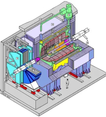
Fig. 6. The L2 Neural Network trigger system, as it is installed within the H1 experiment. The cables on the left carry the information from the various subdetectors to be stored on the receiver cards. The boards in the lower crate (DDB’s) perform the selection and preprocessing of the data, the upper crate holds the CNAPS processor arrays and the control computer.
2) The Data Distribution Board (DDB): Experimental data is received at the trigger system in a variety of formats due to the different characteristics of the readout electronics of the various subdetectors. Before it can be handled by the L2 NN trigger, it
must be reformatted to match the specifications of the CNAPS system. In addition, it may be advantageous to perform cer- tain operations on the raw detector data so as to obtain more salient variables. While it is common in offline NN applica- tions to devote considerable effort to discovering and calculat- ing salient variables to feed the NN, in triggering applications, the realtime aspect severely restricts the complexity of the pre- processing operations which can be performed. In the H1 NN trigger, the functionality of the DDB preprocessor, as described below, is indeed somewhat limited. The upgraded DDB II, to be described in the section III, is much more sophisticated.
The Data Distribution Board resides in a special ”L2 VME crate” equipped with the L2 Bus, an 8 times 16 bit parallel data bus running with the HERA clock in an interleaved mode, yielding an effective 20 MHz transfer rate. For each subdetector the level 1 data are sent serially onto one of the eight subbusses of the L2 backplane. For system control purposes, a special monitor board with an independent readout of the data trans- mitted over the L2 bus resides in the same crate. The data is a heterogeneous mixture from different subdetectors, including calorimetric energy sums, tracker histograms, etc.
On the DDB, the L2 data received are passed through a data type selection where they can be transformed (e. g. split into bytes or single bits) using look-up tables (LUT). After bit split- ting, several preprocessing algorithms like summing of bits and bytes, bit selections or functions can be applied. The data may also be sent unchanged to the selection RAM, where the in- put vector for the neural network computer is stored. Through the use of XILINX 40XX chips the hardware can be flexibly adapted to changes, e.g. for new data formats in the received input. Using selection masks the data are transmitted via a par- allel data bus to a mezzanine receiver card directly connected to the local data bus on the CNAPS board.
D. A Physics Result Using the Neural Trigger
New technologies are never incorporated into working sys- tems solely as an intellectual exercise. The new solution must make some worthwhile contribution to system performance in order to justify the effort and modifications needed to include it.
We present here, summarily, a physics result obtained with the H1 neural trigger, which was unobtainable using the original, non-neural H1 level 2 trigger.
With the trigger system described thus far ([3], see its full realization in fig. 6) data were taken since the summer of 1996.
One of the interesting reactions studied in electron-proton scat- tering is the exclusive production of particles called ‘heavy vec- tor mesons’, e.g., the J/ψ mesons. Measurement of J/ψ pro- duction [6] using the NN trigger has now been carried out over the full kinematic range of HERA, and results have permitted to conclusively rule out what was until now a popular theoretical model for J/ψ production (“Regge-model” [7]).
While it is not appropriate to give here a full account of the
neural networks used to trigger J/ψ production (for details see
[3]), we would nevertheless like to point out the salient fea-
tures of that specific trigger. J/ψ production from an electron-
proton initial state is characterized by the observation of a sin-
gle electron-positron (or muon-antimuon) pair from the J/ψ
decay, the primary beam electron and proton being little de- flected and remaining unobserved in the beam pipe. The de- tector is thus practically “empty” except for these two decay products. At the first level, such events are efficiently triggered by the coincidence of a charged particle track and some en- ergy deposition in the calorimeter, or by two energetic clus- ters. However, since the identical signature is very frequently caused by background processes as well, the level 1 trigger rate is far too high, in certain areas of the detector by up to two orders of magnitude. To cope with the very different back- grounds in the various regions of the detector, the full solid angle of the detector was divided into three parts. For each part a specific network has been optimized offline with real data, two of them in the traditional way using backpropaga- tion, the last one being constructed “by hand” to take into ac- count the simple topological correlations of the decay particles in the very “backward” region of the detector. The input quan- tities for the backpropagation networks were chosen from the proportional chambers (“MWPC”), the drift chambers (“DC”), and the calorimeters. The MWPC information results from the so-called “z-vertex histogram”, which returns statistical estima- tors for a possible event vertex (geometrical interaction point as reconstructed coarsely from track masks by fast coincidence logic). Similarly, the DC’s provide counters at the first trigger level for low and high momentum particle tracks. Finally, the energy depositions in the forward, central and backward parts of the calorimeter were used. A total of typically 10-12 in- puts (64 for the constructed net) were selected. As an exam- ple, the distributions for two typical network input variables are shown in fig. 7: the left figure shows the distribution of the “z- vertex” (resulting from the MWPC trigger processors), both for the signal (open histogram) and the background (shaded his- togram). On the right-hand side the distribution for the number of high momentum, negatively charged particles is shown, as determined from the drift chamber trigger processors. As is visible from the figure, no clear separation is possible between signal and background from these variables alone.
The training samples were obtained from fully reconstructed and positively identified events, both for the background as well as for the signal (which was collected with low efficiency prior to the deployment of the neural network trigger). Since these samples were quite small initially, only a small number of hid- den nodes in the networks could be accepted (typically 4-6 hid- den nodes, where we require, as a “rule-of-thumb”, roughly ten times more training events than free parameters, i.e. weights and thresholds, to be determined). The training was carefully monitored by a control sample (half of the available event sam- ple), thus avoiding overtraining and insufficient approach to the minimum of the error function. Typical background rejections obtained where about 90 percent, with efficiencies of retaining the interesting physics reactions above 95 percent. For the ac- tual data taking at the accelerator the weights determined by the offline training are loaded into the neural hardware and nor- mal recall steps are executed by the neural network trigger to form the event decision. As a general procedure, the networks are re-optimized offline with the additional new data obtained, resulting in better performance.
The NN trigger was thus an essential tool for the measure-
CPVPOS 0
20 40 60 80 100 120
0 10
TRHINEG 0
100 200 300 400 500 600 700
0 5
Fig. 7. Two examples for input quantities to the networks for the signal (J/ψ production, open histogram) and the background (shaded histogram) . Left: distribution of the variable “cpvpos”, a coarse measure of the event ver- tex in the z-direction (“z-vertex”, see text), right: distribution of the number
“trhineg” of negatively charged high momentum particles, as given by the cen- tral drift chambers. The other variables used (not shown here) exhibit similar lack of clear separation between signal and background.
ments of J/ψ production, which were unreachable before the advent of the trigger due to overwhelming background.
III. N EW P REPROCESSING A LGORITHMS : T HE DDB II As HERA will move on to improve its collision rate by a fac- tor of 5 in the year 2003 and beyond, both the H1 detector and its trigger system are being upgraded as well. Since the output rate to tape is to be limited to less than 10 Hz, the H1 trigger sys- tem will face the challenge of even increased rejection power.
In order to meet this goal, the neural network trigger will also be upgraded to improve the preprocessing of the network input to more physics-oriented quantities.
The idea behind this is that the preprocessing will take over
the “trivial” part of the correlations in the trigger data, namely
the association of information from the various subdetectors to
physical objects, as defined by their topological vicinity. Due
to the cylindrical symmetry of H1 about the z axis, data from
any subdetector may be represented graphically on a grid in
z − φ space, where φ is the azimuthal angle. H1 however, uses
a projective coordinate system centered on the collision point,
giving rise to the θ − φ grid of figure 8 (θ is the polar angle) in
which corresponding energy deposits in concentric subdetector
layers are more readily grouped into physical objects. While
with the old DDB I the networks were supplied with quanti-
ties partly integrated over the detector (e.g. energies in certain
topological regions of the detector, numbers of tracks seen in
the drift chambers etc., i.e. global quantities characterizing the
event) the new DDB II finds local physical objects by associ-
ating the information from the various subdetectors, belonging
to the same angular region. These objects are represented by
a vector, the components of which are trigger quantities deter-
mined during the level 1 decision process. With this system, the
full granularity of the level 1 trigger information is exploited,
but the input data volume to the networks is limited to the phys-
ically relevant information.
q j
q - j - region
Fig. 8. Examples of the clustering algorithm in the calorimeter, displaying the θ − φ plane: The algorithm sums up energy depositions which are clustered around local maxima, avoiding double-counting. In this example 5 clusters are found. The remaining energy deposits not associated with clusters are below a preset energy threshold.
A. Preprocessing Algorithms
The central algorithm is clustering in the various subdetec- tors with subsequent matching of the clusters using θ and φ. To be specific, the following steps will be performed in dedicated hardware, making extensive use of fast, modern FPGA technol- ogy:
Cluster Algorithms: The calorimeter will be clustered at the highest available granularity (688 “trigger towers” or TT’s), summing nearest neighbors around a local maximum, as schematically sketched in fig. 8. Double counting of contigu- ous towers is avoided by the algorithm. Before the clustering, look-up tables will perform programmable transformations on the TT energies, for example, calculating the so-called ‘trans- verse energy’, or momentum component measured transversely to the beam direction, taking into account the polar angle θ. For each cluster found, the total energy Etot, the center Ecent with its θ − φ values, the ring energy Ering and the number nhit of towers containing energy above a suitable threshold will be stored.
Bit fields (such as hit maps from the various sets of wire chambers or the trigger cells of the calorimeters) will also be subjected to a cluster algorithm: In this case a preclustering will be performed, summing all immediate neighbors to a given
“seed” bit. After this preclustering, which results in a “hilly”
θ − φ plane, the same algorithm as for the calorimeter will be executed.
Matching: The clusters from the various layers of the de- tector will be gathered in physical objects, forming a vector of which the components represent the list of cluster quanti- ties determined in the previous clustering step. The matching algorithm makes use of the respective θ − φ information. The process is illustrated schematically in fig. 9
Sorting: Subsequently, the objects found will be ordered (‘sorted’) in magnitude according to chosen components. Three parallel sorting machines are foreseen, delivering arrays of vec- tors sorted according to three pre-determined vector compo-
3 lists of paramaters
Counting of objects
Input quantities to the neural network - angular
differences -thresholds Subdetector 1 -...
Subdetector 2
Subdetector 3
Subdetector N ...
clustered data
clustered data
clustered data
clustered data
Clustering Matching Sorting Post processing
Fig. 9. Algorithm to match information from various detector layers to a physical object.
nents like total energy, angular orientation, etc.
Post-processing: An optional final step is also considered which determines some physical quantities from the vector components, such as cluster counting, angular differences etc.
The exact specifications for the post-processing is still under investigation, studying specific physics reactions.
Net Inputs: Due to the serial clocking-in of data into the CNAPS chip, a limit of about 8 to 10 objects (with 8 compo- nents each) plus additional variables from the post-processing step as net input is imposed, which should be quite sufficient for the physics applications considered at present.
As an example of the increased selection power of the DDB II with respect to the less sophisticated DDB presently operating, the production of a second type of ‘heavy vector meson’ called φ has been studied. Using the neural network trigger, this reaction was able to be observed in H1 for the first time[8]. The performance of the NN based on quantities derived from the DDB and expected with the new DDB II is shown in fig. 10. Using the CNAPS for a simulation of the new physics objects to be provided by the DDB II, the selection ef- ficiency - at constant background rejection - could be increased by almost a factor of 2. Further manifestations for the superior separating power of the DDB II in more complicated reactions have been obtained in simulations.
It should be stressed here once more that the improved net- work performance observed with the DDB II is the result of a more intelligent use of the available input information: The preprocessing determines correlations among the trigger quan- tities, which could, in principle, also be found by a sufficiently complex network, given a correspondingly increased data set and adequate computing time for the offline training. In our concrete trigger example, however, large training samples are not available and therefore the “brute force” scenario is ex- cluded. It is not surprising that physically motivated, cleverly prepared variables (i.e. an intelligent data reduction scheme) help tremendously in improving the neural network perfor- mance.
B. Hardware Implementation
The hardware implementation of the DDB II system can be
divided into two parts, a control and the signal processing unit
output: background
0 0.2 0.4 0.6 0.8 1
0 2 4 6 8 10 12 14 16 18 20
output: signal
0 0.2 0.4 0.6 0.8 1
0 2 4 6 8 10 12 14 16 18 20 22
background efficiency
0 0.2 0.4 0.6 0.8 1
signal efficiency
0 0.2 0.4 0.6 0.8 1
output: background
0 0.2 0.4 0.6 0.8 1
0 10 20 30 40 50 60 70 80
output: signal
0 0.2 0.4 0.6 0.8 1
0 10 20 30 40 50
background efficiency
0 0.2 0.4 0.6 0.8 1
signal efficiency
0 0.2 0.4 0.6 0.8 1
DDB I DDB II
Fig. 10. Output distributions for a network trained to select φ-mesons, using inputs obtained from the DDB (left) and DDB II (right). The lower diagrams show the efficiencies to reject background as functions of the output cut (ab- scissa is the cut, ordinate the efficiencies). All data are obtained from real running at the accelerator. The curves for DDB II are obtained from a simu- lation of the respective quantities on the CNAPS, which was possible for the simple case of φ production. The clear improvement of discrimination power using the DDB II is evident.
as shown in fig. 11. Like all other data processing equipment at the H1 experiment the DDB II system is controlled via a VME- bus system. Each access to a VME-resource on the DDB II board proceeds under the control of the VME-bridge device.
This device is also responsible for the initialization and the monitoring of all other FPGA-devices on the printed circuit board.
The signal processing path of the DDB II system starts with the L2 bus interface. The L2 Data Translation Table (LDTT) device gives the opportunity to transform the data via L2 bus through pre-loadable lookup tables. The functionality of the old DDB system is for compatibility reasons also integrated in this device. The translated data samples are then distributed to the different clustering engines. Next, the clustered subdetector data are combined to physical objects in the matching unit. The last two steps, the ordering and post-processing will be done in the CNAPS-CTRL device, which also controls the interaction with the associated CNAPS board. This device also generates the L2 trigger decision following the network operation. For a detailed description of the L2 hardware scheme with the DDB II
Mem
Mem
Mem
Mem Clustering subdetector 1
Clustering subdetector 2
Clustering subdetector
Clustering subdetector N
Matching Data Addresses L2 bus
VME bridge Z8-Core Flash
LDTT DDB1 Preprocessor
CNAPS
C N A P S C on tr ol
VME bus
to L2 Trig
...
Fig. 11. Structure of the DDB2 system
system see [10].
IV. N EW A RCHITECTURES FOR N EURAL N ETWORK
T RIGGERS OF U PCOMING E XPERIMENTS
After the upgrade of the data pre-processing stage for the H1 neural network trigger, interest will focus on the improvement of the intrinsic neural network hardware implementation, espe- cially since the CNAPS chip has not seen an architectural revi- sion for many years and in any case is no longer manufactured.
Another strong motivation for exploring more advanced im- plementations of neural network triggers is the new round of experiments planned for the LHC facility under construction at CERN. Multi-level trigger systems for the large colliding-beam experiments ATLAS [11] and CMS [12] at LHC have been pro- posed, similar to the ones existing now at HERA.
For ATLAS, as an example, the planned first trigger level comes from the calorimeter or outer tracking chambers, real- ized in dedicated hardware, with a typical latency of about 2 µs. During this decision time the detector information is stored deadtime-free in so-called pipelines for final readout. One of the important tasks of the first level calorimeter trigger is to detect single, isolated particles exiting with very high trans- verse energy, in an environment dominated by the emission of many tight bundles of particles called “jets”. A fast neural net- work analyzing the patterns of energy clusters in the calorimeter would be an ideal tool to match this challenging task.
In what follows, the ATLAS experiment has served as a ‘test scenario’ for the development of two new neural trigger ar- chitectures obeying realistic constraints for a first-level trig- ger: number of inputs of order 100 (representing individual calorimeter cells in a 3-dimensional array around a cluster cen- ter); ability to accept a new set of inputs every BC (25 ns);
and a latency of the neural operation of the order of 500 ns.
The first architecture presented deals with a parallel dataflow
combined with standard arithmetic data processing, while the
second, ‘Dolfin’, is based on a serial arithmetic data process-
ing scheme. A third subsection presents a comparison of the
performance of the two architectures on specific problems, and
in subsection D, a brief summary of other hardware options is
given.
A. Very Fast Parallel Neural Network Architecture for Level 1 Triggering
1) Context of Level 1 Triggering: As neural networks have proven to be powerful processing tools at level 2, it is natural for physicists to ask whether they might also benefit from them at level 1. Aside from a few test experiments implementing neural networks at L1, however, this idea has not significantly advanced because available digital technology was unable to meet the timing constraints [13]. In light of recent advances, however, it is interesting to now re-examine this question.
To illustrate what may be possible today, a trigger scheme based on a dedicated fast neural chip is presented. The trig- gering specifications were based on those of the level 1 in the ATLAS experiment at LHC, that is, data arriving at each bunch crossing (25 ns), and a latency of (nominally) 500 ns is available to perform all of the neural processing. The chip architecture was developed at the Laboratoire des Instruments et Syst`emes d’Ile de France, in a collaboration with the Max Planck Institut f¨ur Physik in Munich.
The neural network is the principal element of the trigger. It exploits data coming from the ATLAS calorimeter in order to perform optimal particle identification. Four classes of particles are allowed (for example, electron, photon, muon, jet), which thus fixes the number of outputs of the neural network at four.
A study of the specifications of proposed calorimeter triggers led to a choice of 128 inputs to the net. This could correspond, for example, to the number of cells belonging to a local area with an 8 ∗ 8 granularity around a specific tower in two consec- utive layer of a sub-detector. It is worth noting that although the NN architecture thus obtained resembles closely those used in the level 2 applications discussed earlier, its function is rather different, performing a local particle identification task rather than a global event accept/reject decision. In addition, level 2 triggers do not need to be able to accept new data at each bunch crossing.
While the numbers of inputs to and outputs from the neu- ral network are determined by the physical requirements in the task to be performed (here: classification of three-dimensional shower patterns in a fine-grain calorimeter, returning probabil- ities for four particle classes), there is no firm general rule for the number of neurons and their topological arrangement in the hidden layers. As mentioned above, a guideline is provided by the offline training process, where the size of the training sam- ple yields an estimate of the number of free parameters which could possibly be constrained during the backpropagation al- gorithm. Given sufficient statistics, however, a heuristic ap- proach suggests a number of hidden nodes (in a single hidden layer) of roughly the same size as the number of input nodes. In our concrete example of a pattern recognition machine for the calorimeter trigger of ATLAS we have selected, given the se- vere time constraints in the execution phase, a hidden layer with 64 nodes. For the offline training, the complexity of such a net- work is quite high, but still manageable with present-day com- puting environments. Since it is foreseen to use Monte Carlo simulations of shower patterns, statistics is not a limiting fac- tor.
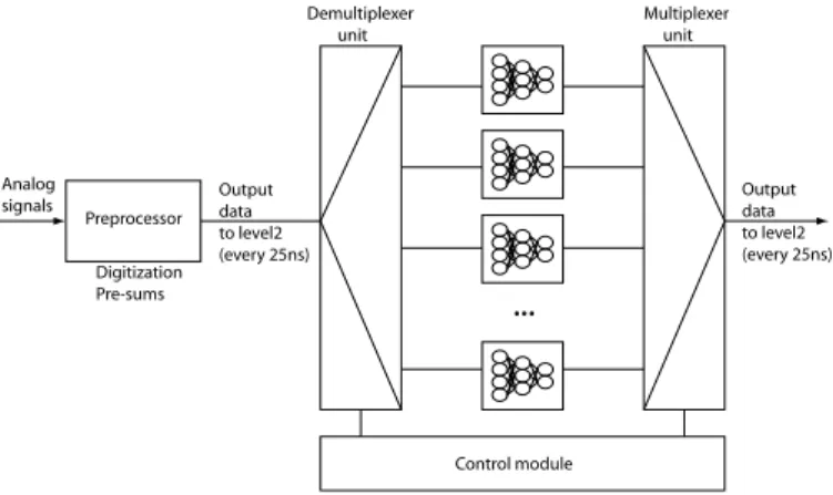
A description of the trigger scheme is given in figure 12. The central processing section consists of a neuro-chip which imple-
Demultiplexer unit
Multiplexer unit
Control module Preprocessor
Digitization Pre-sums Analog
signals Output
data to level2 (every 25ns) Output
data to level2 (every 25ns)
...
Fig. 12. The triggering scheme
ments the overall structure of the neural network. The incom- ing analog data collected in the sub-detectors pass through a pre-processing unit which performs the digitization and applies straightforward manipulations to make them exploitable by the neuro-chips. A demultiplexing unit sequentially distributes the signals to the neuro-chips in a time-multiplexed way. This con- figuration permits to perform many more computations by con- sidering the total latency time of 500 ns and not simply the small processing time available between two collisions (25 ns).
These neuro-chips are replicated, and each implements exactly the same neural network. Finally, a multiplex unit recombines the outputs of the neuro-chips and sends them serially to the central trigger logic.
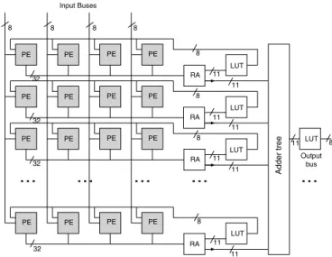
2) Description of the Individual NN Circuits: The proposed architecture adopts a strategy of massive parallelism in order to address the difficult challenge of processing the data within the timing range imposed by level 1. It consists of a matrix dis- tribution of simple processing elements (PE) which perform the total computation in a parallel way. The architecture is depicted in figure 13, while a detailed description of a single PE is given in figure 14.
Since the number of outputs of the neural network is fixed to 4 in this configuration, the processors matrix is composed of 4 columns. The number of rows corresponds to the number of neurons to be computed in the hidden layer. Fixed-point nota- tion was chosen for the basic data representation. The weights are coded in 16 bits and the outputs in 8 bits, which is ade- quate for most neural network implementations [14]. Each PE contains an internal memory to store the weights and a set of additional registers to store possible intermediate results. The memories allow to store a maximum of 64 words of 16 bits each. These values were chosen as being the most appropriate for our specific configuration. A Multiplication ACcumulation unit (MAC) performs the sum of products in 32 bits, for the evaluation of the neuron activities. The impact of different data codings has not been simulated, as the real specifications of the application are not yet completely known. The proposed de- fault values were retained since they correspond to an optimal use of the available logic resources. However, the circuit was designed to keep a high flexibility, and data coding may easily be changed due to implementation in reconfigurable devices.
All PE units are managed by a main internal control module
PE PE PE PE RA
LUT
PE PE PE PE
RA LUT
PE PE PE PE
RA LUT
PE PE PE PE
RA LUT
... ... ... ... ...
LUT
A dder tree
Input Buses
Output bus
8 8 8 8
11
32
32 32 32
11
11
11
8
11 11 11 11
11 8
8
8
8
Fig. 13. Architecture of the neuro-processor
Address Generator
Multiplier Accumulator
Weights Memory
Data bus (in) Data bus (out)
command bus Input data
Register bank
Fig. 14. Description of a Processing Element
consisting of a state machine steered by a command bus. Each line of 4 PE’s ends with a Row Accumulator unit whose pur- pose is to combine the different pre-sums coming from all PE’s within the corresponding row. This unit is composed of a 32 bit accumulator and of a truncation unit enabling to pass from the 32 bit precision to 11 bits. This last value corresponds to the size of the address bus connected to the tables in which the activation function is stored.
Each row of PE’s contains an internal memory whose role is to store the values of the output function. These memories consist of 18 kbit RAMs and allow the storage of up to 2048 values of 9 bits. These values however may be easily configured depending on the precision desired.
An Input/Output module distributes the incoming data on 4 parallel input buses each of which addresses a column of PE’s separately. After complete processing, the data are sent seri- ally via an output bus to the same module. Computations are performed in several steps :
• First, 4 out of the 128 inputs are provided at every clock cycle on the 4 input parallel buses and are accessible to all PE’s at the same time. Each PE performs a MAC opera- tion and stores the results in an internal register. This op- eration is repeated until all input data are processed which occurs after 32 clock cycles. The input layer calculation is performed using neuron parallelism, i.e., 32 subsequent
incoming weights to a neuron are partially stored within the corresponding PE internal memory.
• The different pre-sums are then accumulated within a row and address the associated LUT in which the output func- tion is stored. At this point, all units in the hidden layer are processed and the different neuron outputs are then avail- able to compute the output layer.
• The next step consists in broadcasting the neuron outputs back to all PE’s within each row. In this configuration, each PE belonging to a column computes a part of the activity of one output neuron using synapse parallelism.
The sub-results from each PE within a column have to be added. The pipelined adder tree collects the different sub- results and sequentially provides the results. The output of the last adder is directly connected to a memory in which the activation function is stored.
• The outputs of the neural network are then sent serially to the input/output module for communication with the ex- ternal world.
The architecture was designed to guarantee a very high exe- cution speed. Beyond the massive parallelism, the way in which the different computations overlap is also crucial. For example, the circuit may begin to read a new input vector while process- ing the last vector. Table II shows that the execution time is 50 clock cycles, that is to say that the entire neural network is completely computed after this latency. The computational overlap consists in taking advantage of the fact that all PE’s are partially available after computation of the first post-synaptic product, i.e., 32 clock cycles. After that time, new data are then ready to be processed, without disturbing other computations.
We qualify this by remarking that the hidden layer computation may sometimes be interrupted during the output layer computa- tion; however, this operation is very short and does not generate any significant delay or freezing in the computation process.
Table I presents the execution time according to the number of inputs. The function tends to be linear when the number of inputs is sufficiently large. For a small number of inputs, this behavior is no longer observed. This is mainly due to a certain number of operations whose timing execution is independent of the number of inputs (e.g memory reading, data transfers on the bus, or operation latency).
One of the main advantages of the design is that the tim- ing execution of the entire neural network is independent of the number of hidden units. In fact, this feature was the motivat- ing factor in the conception and architectural choices, since the latency constraint was the most stringent. The price to be paid for this of course is a strong dependence on the required logical resources. Table II shows the timing dependence as a function of the number of hidden units.
The main drawback of our architecture is the correlation
between the number of multipliers and the number of hidden
units. Each PE contains a multiplier and since there are 4 PE
within a row, the maximum number of hidden units which are
effectively computable is N M U L/4 where N mul is the total
number of required multipliers in the device. Since this arith-
metic operation is the most demanding in terms of resources, it
is obvious that the use of dedicated multipliers is unavoidable
in order to save logic resources.
Number of inputs Number of clock cycles
4 19
8 20
16 21
32 26
64 34
128 50
TABLE I
T IMING EXECUTION AS A FUNCTION OF THE NUMBER OF INPUTS
Number of Number of clock hidden units cycles
4 46
8 47
16 48
32 49
64 50
TABLE II
T IMING EXECUTION AS A FUNCTION OF THE NUMBER OF HIDDEN UNITS
A further consideration is the execution time as a function of the number of outputs. Table III shows a quasi-linear func- tion starting from a small number of outputs. The output layer computation being pipelined, it is rather normal to observe this linearity. This result, however, is only an estimation and does not take into account the size of the register bank within a PE.
Such banks are useful for example for storing intermediate re- sults. A problem that may occur in case of an increase of the number of outputs is the introduction of delays in the compu- tation, which has an impact on the recovery of computations.
Indeed, each PE is only capable of executing a single multipli- cation within a clock cycle, and cannot process this operation for both hidden layer and output layer at the same time.
Another important feature of our design is its relatively small number of inputs and outputs. Only 75 pins are necessary to im- plement the 128-64-4 network, which considerably simplifies connectivity and board implementation. Moreover, the massive parallelization of calculations implies that it is possible to in- crease the size of the network to be implemented by cascading more chips, which will not drastically affect the timing perfor- mance.
Since it seemed unnecessary to implement learning algo- rithms in case of triggering applications, this feature has not been retained. Nevertheless, it could be imagined to imple- ment such a feature thanks to our choice of FPGA’s with their intrinsic flexibility and reconfiguration properties. One might, for example, reconfigure the FPGA between the execution and back-propagation phase of the learning algorithm.
3) Hardware Implementation: Our final circuit must be able to implement a 128-64-4 MLP in 500 ns. It has been shown in [9] that FPGA devices are the most appropriate for imple- menting neural network architectures with tight timing con- straints, most importantly because of the possibility of mas-
sively parallel computation to limit the number of execution cycles. FPGA’s, furthermore, ensure the flexibility to modify the circuit over time if need be; after implementing a baseline configuration corresponding to a specific size of network, for example, one could later reconfigure the FPGA if the specifica- tions changed, simply by downloading the configuration onto the hardware itself. A third reason for the choice of FPGA’s is the possibility to take advantage of internal resources which are particularly suited to the application. For example, FPGA’s enable to implement a significant number of storage elements, such as memories or registers, which are very useful for storing weights, activation functions, etc. In circuits with fewer intrin- sic storage elements, it is often necessary to provide external memories with correspondingly longer access times, thus de- grading the overall performance of the system.
These motivations have led to the choice of the Xilinx Vir- tex II family [15] for our circuit, as it is the only one with adequate speed performance and a sufficient number of inter- nal multipliers to implement the design architecture. The target chip, the XC2V-8000, is the largest available today, providing 8 Million equivalent gates, as well as 168 18 ∗ 18 bit embedded multipliers and their associated internal block memories, which will be particularly valuable in the case of massively parallel computations. Table IV shows the number of embedded multi- pliers used for different sizes of networks. In this table, it can be clearly seen that for the target chip, above 42 hidden units, it is necessary to build multipliers within logic cells, as all dedicated blocks are already used. In this case, a considerable amount of logic resources is devoted to these remaining multiplication op- erations, which may significantly increase the complexity of the design.
After synthesis and implementation, it was found that only
70% of the logic resources of the FPGA were utilized. This
Number of neurons in Number of clock the output layer cycles
4 50
8 54
12 58
16 62
20 66
TABLE III
T IMING EXECUTION AS A FUNCTION OF THE NUMBER OF OUTPUTS
Network Size Number of Number of dedicated Number of utilized Percentage of Inputs/Outputs multipliers memory blocks logic resources
128-4-4 75 16 5 4
128-8-4 75 32 9 7
128-16-4 75 64 17 14
128-32-4 75 128 33 25
128-42-4 75 168 43 33
128-64-4 75 168 65 70
TABLE IV
I MPLEMENTED NETWORKS AND UTILIZED RESOURCES
however is acceptable in light of the fact that in FPGA design, it is not always recommended to fill the circuit more than 80
%, in order to avoid performance degradation due to routing delays. As for sequential processing, we verified that only 50 clock cycles were necessary to process the entire neural net- work. Furthermore, in this configuration, only 32 cycles are required before processing a new input pattern. A timing sim- ulation showed that a clock frequency of 120 MHz could be be reached, indicating that the specifications can be met using current programmable technology.
The simulation results of the FPGA solution, which uses
‘standard arithmetic’, as well as a comparison to ‘Dolfin’ (see below) and to CNAPS, are presented in section IV.C and ta- ble VIII.
B. Dolfin - Digit Online for Integration Neural Networks As another possible option for the individual NN’s in figure 12, we have also considered a serial arithmetic approach. In large network structures the efforts to interconnect the neurons becomes of increasing significance. One possible solution to this problem is a serial data transmission between the network elements. Once a serial data stream for the interconnections is used, there is no need for parallel to serial and reverse conver- sion, since the internal calculation of a neuron by efficient serial arithmetic exists. This has been explained in [16] as follows.
The necessary functions for the implementation of a neuron can be divided into three different phases: the input weight- ing, the weighted input summation and the calculation of the neuron output signal. The first two functions can be easily im- plemented by ordinary multiplication and addition operations.
Only the realization of the output function calculation requires a complex hardware implementation.
The most commonly utilized functions in this field are the so called sigmoid function, defined by f (x) = 1/(1 + e −x ), and the tanh function, defined by f (x) = (e x − e −x )/(e x + e −x ).
Usually these functions are implemented by lookup tables with an implementation effort depending strongly on the requested accuracy. For a serial data processing system, a digit-online algorithm [18] based approximation of the tanh output func- tion, as first presented in [16], can reduce the hardware efforts and speed up the performance of a serially implemented neuron function without any impact to the network behavior.
Unlike most other serial arithmetic implementations, digit- online algorithms generate results starting with the most signif- icant digit (MSD) first. This is possible due to the utilization of a redundant number system. A signed-digit representation, described by eqn. 1, is used here, but carry-save is also possible.
X =
j+σ
X
i=0
x i r −i with {x i } ∈ {−p, . . . , −1, 0, 1, . . . , p}
and r
2 ≤ p ≤ r − 1 (1)
In this case the term “redundant” characterizes the utilization of a redundant number system for the number representation and does not refer to the robustness of the arithmetic circuit against internal failure. Like non-redundant number systems the base value r of the number representation can be freely cho- sen. With a given number base r = 2 in eqn. 1 the commonly utilized redundant binary number system allows the digit values
¯ 1, 0, 1.
A value can have many different signed digit (SD) vector
equivalences due to the redundant number representation. As
an example the value 3 can have the following representations
in a 4-digit vector 0011, 010¯ 1 , 01¯ 11, 1¯ 10¯ 1, 1¯ 1¯ 11. The multiple representation of one value may pose some problems if one must detect a particular value such as in a comparator. In such a case one must first transform the redundant number represen- tation into a non-redundant system. This can be done simply with an ordinary carry propagate adder (CPA).
As for the non-redundant number system, in a redundant number scheme we have also an adder structure as a basic module for more complex operations. The main advantage of such a redundant adder (RA) is a constant delay independent of operand length. The behavior of such a signed digit adder can be described by table V and table VI. The idea of this redundant adder is to prevent a possible overflow in table VI by generation of a speculative carry in table V.
x i , y i x i − 1 , y i − 1 u i z i
{11} 1 0
{10, 01} {01, 10, 11} 1 ¯ 1 { ¯ 11, 00, 1¯ 1} 1 ¯ 1 {0¯ 1, ¯ 10, ¯ 1¯ 1} 0 1 { ¯ 11, 00, 1¯ 1} {01, 10, 11} 0 0 { ¯ 11, 00, 1¯ 1} 0 0 {0¯ 1, ¯ 10, ¯ 1¯ 1} 0 0 { ¯ 10, 0¯ 1} {01, 10, 11} 0 ¯ 1 { ¯ 11, 00, 1¯ 1} ¯ 1 1 {0¯ 1, ¯ 10, ¯ 1¯ 1} ¯ 1 1 { ¯ 1¯ 1} ¯ 1 0
TABLE V
SD ADDER LOGIC TABLE PREPROCESSING
u i− 1 , z i s i
{11} not def.
{10, 01} 1 { ¯ 11, 00, 1¯ 1} 0 { ¯ 10, 0¯ 1} ¯ 1
{ ¯ 1¯ 1} not def.
TABLE VI
SD ADDER LOGIC TABLE POSTPROCESSING
Unfortunately the implementations of redundant adders like the Takagi adder [17] shown in Fig. 15 for SD operands are slightly larger than non-redundant adders.
Simple arithmetic functions like addition or multiplication can be implemented easily without the utilization of redun- dant adders in a least significant digit (LSD) first manner. An MSD-first implementation is also possible when using redun- dant adder structures. Higher level arithmetic operations like division or square root are MSD-first algorithms by nature; they cannot be transformed to a LSD-first style without an extreme performance penalty.
To determine the optimal direction of the serial data trans- mission we have to examine the internal processing operations of a neuron. If we limit the implementation only to the intrinsic
1 2
3 5
6
4 7
X1S Y1S
P V
SS SD VA
PA X1D Y1D
Fig. 15. SD Takagi adder
data processing path, then we have a multiplication for the input weighting, some additions for the summation of the weighted inputs, and a classification operation. Depending on the type of classification function different operations will be involved. In our approach we focus on the use of a sigmoid or tanh function for the classification in a feedforward network architecture. To prevent a performance bottleneck in the serial communication, we must not utilize lookup table based solutions. Furthermore we need a similar operation mode for all serial modules, either all modules using a least significant digit (LSD) first data result generation and transmission, or a most significant digit (MSD) first behavior. Due to the loss of time during the conversion of one transmission type into the other, we must not mix types in a single circuit, as shown in Fig. 16. Hence, we must de- termine the least common denominator for the possible trans- mission type. For the mult and add operations, both LSD and MSD implementations exist, but for the classification operation we need a MSD-type communication as shown in Fig. 17.
serial transmission
sequential processing
Op n−1 Op
n Op
n+1
serial transmission
MSD √ LSD
+
LSD
*
LIFO LIFO
serial transmission
Op n−1 Op
n Op
n+1
serial transmission
MSD √ LSD
+
LSD
*
LIFO LIFO
Fig. 16. Performance bottleneck through transmission direction conversion in a mixed LSD and MSD scheme
The digit online arithmetic represents such a possible family of MSD-first algorithms, which was first presented in [19].
The idea of digit-online algorithms can be described for a two operand example with eqn. 2-3 and the following iteration given by eqn. 4.
S = f (X, Y ) with X =
j+δ
X
i=0
x i r −i ; Y =
j+δ
X
i=0
y i r −i (2)
{x i , y i , s i } ∈ {−p, . . . , −1, 0, 1, . . . p}
serial transmission
sequential processing
Op n−1 Op
n Op
n+1
serial transmission
MSD MSD √
+
MSD
* LSD...MSD LSD...MSD
serial transmission
Op n−1 Op
n Op
n+1
serial transmission
MSD MSD √
+
MSD
* LSD...MSD LSD...MSD
Fig. 17. Optimized throughput in a pure MSD transmission scheme
and r
2 ≤ p ≤ r − 1 Initialization:
W ( −δ+1 ... − 1) ← C X 0 ← 0 (3) s ( − δ ... − 1) ← 0 Y 0 ← 0
Recursion:
for j = 0, 1, . . . , m W j ← (W j − 1 − s j − 1 ) +
f (x − δ , x j , X(j − 1), y j , Y j− 1 ) (4) s j − 1 ← S(W j )
and the selection function:
S (W j ) =
r − 1, if w s < W j
0, if −w s ≤ W j ≤ w s
−r − 1, if W j < w s
(5)
The algorithm starts with an initialization of some variables, the scaled residual W j , the operand vectors X j and Y j , and the first δ-result digits s. Depending on the function, the algo- rithm needs δ leading operand-digits to calculate the first result digit. This incorporates a function specific online delay δ for the result generation. During the following recursion the ac- tual residual W j will be calculated and each iteration outputs a new result digit s j determined by the selection function eqn. 5.
The resulting digit vector approximates the result step-by-step as shown in Fig. 18. The redundant number system allows any necessary corrections of a previously estimated result.
As an example we will demonstrate the behavior of a simple digit online algorithm. A digit online addition can be described by eqn.6..8 for a minimal redundant binary number system with r = 2, p = 1.
Initialization:
W − 1 ← 0 X 0 ← 0 (6)
s − 1 ← 0 Y 0 ← 0
Recursion:
for j = 0, 1, . . . , m + 1
W j ← (W j − 1 − s j − 2 ) + r −δ (x j + y j ) (7) s j − 1 ← S(W j )