MicroBlaze Processor
Reference Guide
Embedded Development Kit EDK 10.1i
UG081 (v9.0)
possible implementation of this feature, application, or standard, Xilinx makes no representation that this implementation is free from any claims of infringement. You are responsible for obtaining any rights you may require for your implementation. Xilinx expressly disclaims any warranty whatsoever with respect to the adequacy of the implementation, including but not limited to any warranties or representations that this implementation is free from claims of infringement and any implied warranties of merchantability or fitness for a particular purpose.
MicroBlaze Processor Reference Guide UG081 (v9.0)
The following table shows the revision history for this document.
Date Version Revision
10/01/02 1.0 Xilinx EDK 3.1 release 03/11/03 2.0 Xilinx EDK 3.2 release 09/24/03 3.0 Xilinx EDK 6.1 release 02/20/04 3.1 Xilinx EDK 6.2 release 08/24/04 4.0 Xilinx EDK 6.3 release
09/21/04 4.1 Minor corrections for EDK 6.3 SP1 release 11/18/04 4.2 Minor corrections for EDK 6.3 SP2 release 01/20/05 5.0 Xilinx EDK 7.1 release
04/02/05 5.1 Minor corrections for EDK 7.1 SP1 release 05/09/05 5.2 Minor corrections for EDK 7.1 SP2 release 10/05/05 5.3 Minor corrections for EDK 8.1 release 02/21/06 5.4 Corrections for EDK 8.1 SP2 release 06/01/06 6.0 Xilinx EDK 8.2 release
07/24/06 6.1 Minor corrections for EDK 8.2 SP1 release 08/21/06 6.2 Minor corrections for EDK 8.2 SP2 release 08/29/06 6.3 Minor corrections for EDK 8.2 SP2 release 09/15/06 7.0 Xilinx EDK 9.1 release
02/22/07 7.1 Minor corrections for EDK 9.1 SP1 release 03/27/07 7.2 Minor corrections for EDK 9.1 SP2 release 06/25/07 8.0 Xilinx EDK 9.2 release
10/12/07 8.1 Minor corrections for EDK 9.2 SP2 release
01/17/08 9.0 Xilinx EDK 10.1 release
Preface: About This Guide
Guide Contents . . . 5
Conventions . . . 6
Typographical . . . 6
Online Document . . . 7
Chapter 1: MicroBlaze Architecture Overview . . . 10
Features . . . 10
Data Types and Endianness . . . 12
Instructions . . . 13
Registers . . . 21
General Purpose Registers . . . 21
Special Purpose Registers . . . 22
Pipeline Architecture . . . 44
Three Stage Pipeline . . . 44
Five Stage Pipeline . . . 44
Branches . . . 44
Memory Architecture . . . 46
Privileged Instructions . . . 47
Virtual-Memory Management . . . 48
Real Mode . . . 48
Virtual Mode . . . 49
Translation Look-Aside Buffer . . . 50
Access Protection . . . 55
UTLB Management . . . 56
Recording Page Access and Page Modification . . . 57
Reset, Interrupts, Exceptions, and Break . . . 58
Reset . . . 58
Hardware Exceptions . . . 59
Breaks . . . 61
Interrupt . . . 62
User Vector (Exception) . . . 62
Instruction Cache . . . 63
Overview . . . 63
General Instruction Cache Functionality . . . 63
Instruction Cache Operation . . . 64
Instruction Cache Software Support . . . 64
Data Cache . . . 65
Overview . . . 65
General Data Cache Functionality . . . 65
Data Cache Operation . . . 66
Data Cache Software Support . . . 66
Floating Point Unit (FPU) . . . 67
Operations . . . 68
Exceptions . . . 68
Fast Simplex Link (FSL) . . . 69
Hardware Acceleration using FSL . . . 69
Debug and Trace . . . 70
Debug Overview . . . 70
Trace Overview . . . 70
Chapter 2: MicroBlaze Signal Interface Description Overview . . . 71
Features . . . 71
MicroBlaze I/O Overview . . . 72
Processor Local Bus (PLB) Interface Description . . . 77
On-Chip Peripheral Bus (OPB) Interface Description . . . 77
Local Memory Bus (LMB) Interface Description . . . 77
LMB Signal Interface . . . 78
LMB Transactions . . . 80
Read and Write Data Steering . . . 82
Fast Simplex Link (FSL) Interface Description . . . 83
Master FSL Signal Interface . . . 83
Slave FSL Signal Interface . . . 83
FSL Transactions . . . 84
Direct FSL Connections . . . 84
Xilinx CacheLink (XCL) Interface Description . . . 85
CacheLink Signal Interface . . . 86
CacheLink Transactions . . . 87
Debug Interface Description . . . 89
Trace Interface Description . . . 89
MicroBlaze Core Configurability . . . 92
Chapter 3: MicroBlaze Application Binary Interface Data Types . . . 97
Register Usage Conventions . . . 98
Stack Convention . . . 99
Calling Convention . . . 101
Memory Model . . . 101
Small Data Area . . . 101
Data Area . . . 101
Common Un-Initialized Area . . . 101
Literals or Constants . . . 101
Interrupt and Exception Handling . . . 102
Chapter 4: MicroBlaze Instruction Set Architecture Notation . . . 103
Formats . . . 104
Instructions . . . 105
Preface
About This Guide
The MicroBlaze™ Processor Reference Guide provides information about the 32-bit soft processor, MicroBlaze, which is part of the Embedded Processor Development Kit (EDK). The document is intended as a guide to the MicroBlaze hardware architecture.
Guide Contents
This guide contains the following chapters:
• Chapter 1, “MicroBlaze Architecture”, contains an overview of MicroBlaze features as well as information on Big-Endian bit-reversed format, 32-bit general purpose registers, cache software support, and Fast Simplex Link interfaces.
• Chapter 2, “MicroBlaze Signal Interface Description”, describes the types of signal interfaces that can be used to connect MicroBlaze.
• Chapter 3, “MicroBlaze Application Binary Interface”, describes the Application Binary Interface important for developing software in assembly language for the soft processor.
• Chapter 4, “MicroBlaze Instruction Set Architecture”, provides notation, formats, and instructions for the Instruction Set Architecture of MicroBlaze.
For additional information, go to http://support.xilinx.com. The following table lists some of the resources you can access directly using the provided URLs.
Resource Description/URL
Tutorials Tutorials covering Xilinx
®design flows, from design entry to verification and debugging.
http://support.xilinx.com/support/techsup/tutorials/index.htm Answer Browser Database of Xilinx solution records.
http://support.xilinx.com/xlnx/xil_ans_browser.jsp
Application Notes Descriptions of device-specific design techniques and approaches.
http://www.xilinx.com/xlnx/xweb/xil_publications_index.jsp?category=
Application+Notes
Data Book Pages from The Programmable Logic Data Book, which contains device- specific information on Xilinx device characteristics, including readback, boundary scan, configuration, length count, and debugging.
http://support.xilinx.com/xlnx/xweb/xil_publications_index.jsp
Problem Solvers Interactive tools that allow you to troubleshoot your design issues.
Conventions
This document uses the following conventions. An example illustrates each convention.
Typographical
The following typographical conventions are used in this document:
Tech Tips Latest news, design tips, and patch information for the Xilinx design environment.
http://www.support.xilinx.com/xlnx/xil_tt_home.jsp GNU Manuals The entire set of GNU manuals.
http://www.gnu.org/manual
Resource Description/URL
Convention Meaning or Use Example
Courier font Messages, prompts, and program
files that the system displays. speed grade: - 100 Courier bold Literal commands that you enter
in a syntactical statement. ngdbuild design_name
Helvetica bold
Commands that you select from a
menu. File → Open
Keyboard shortcuts Ctrl+C
Italic font
Variables in a syntax statement for which you must supply values.
ngdbuild design_name References to other manuals. See the Development System
Reference Guide for more information.
Emphasis in text. If a wire is drawn so that it overlaps the pin of a symbol, the two nets are not connected.
Square brackets [ ]
An optional entry or parameter.
However, in bus specifications, such as bus[7:0] , they are required.
ngdbuild [option_name]
design_name
Braces { } A list of items from which you
must choose one or more. lowpwr ={on|off}
Vertical bar | Separates items in a list of
choices. lowpwr ={on|off}
Online Document
The following conventions are used in this document:
Convention Meaning or Use Example
Cross-reference link to a location in the current document
See the section “Additional Resources” for details.
Refer to “Title Formats” in Chapter 1 for details.
Cross-reference link to a location in another document
See Figure 2-5 in the Virtex-II Handbook.
Hyperlink to a web-site (URL) Go to http://www.xilinx.com for the latest speed files.
Vertical ellipsis . . .
Repetitive material that has been omitted
IOB #1: Name = QOUT’
IOB #2: Name = CLKIN’
. . . Horizontal ellipsis . . . Repetitive material that has been
omitted
allow block block_name loc1 loc2 ... locn;
Convention Meaning or Use Example
Blue text
Red text
Blue, underlined text
Chapter 1
MicroBlaze Architecture
This chapter contains an overview of MicroBlaze™ features and detailed information on
MicroBlaze architecture including Big-Endian bit-reversed format, 32-bit general purpose registers, virtual-memory management, cache software support, and Fast Simplex Link (FSL) interfaces.
This chapter has the following sections:
• “Overview”
• “Data Types and Endianness”
• “Instructions”
• “Registers”
• “Pipeline Architecture”
• “Memory Architecture”
• “Privileged Instructions”
• “Virtual-Memory Management”
• “Reset, Interrupts, Exceptions, and Break”
• “Instruction Cache”
• “Data Cache”
• “Floating Point Unit (FPU)”
• “Fast Simplex Link (FSL)”
• “Debug and Trace”
Overview
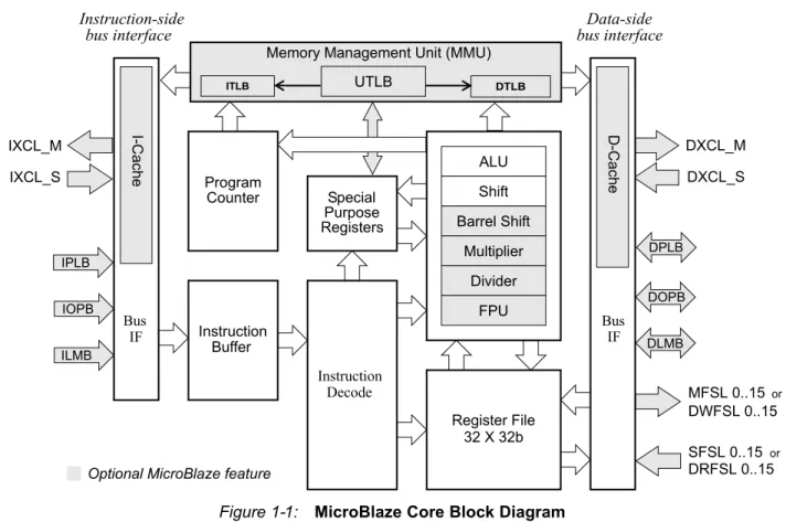
The MicroBlaze™ embedded processor soft core is a reduced instruction set computer (RISC) optimized for implementation in Xilinx
®Field Programmable Gate Arrays (FPGAs). Figure 1-1 shows a functional block diagram of the MicroBlaze core.
Features
The MicroBlaze soft core processor is highly configurable, allowing you to select a specific set of features required by your design.
The fixed feature set of the processor includes:
• Thirty-two 32-bit general purpose registers
• 32-bit instruction word with three operands and two addressing modes
• 32-bit address bus
• Single issue pipeline
In addition to these fixed features, the MicroBlaze processor is parameterized to allow selective enabling of additional functionality. Older (deprecated) versions of MicroBlaze support a subset of the optional features described in this manual. Only the latest (preferred) version of MicroBlaze (v7.10) supports all options.
Xilinx recommends that all new designs use the latest preferred version of the MicroBlaze processor.
Table 1-1, page 11 provides an overview of the configurable features by Microblaze versions.
Figure 1-1: MicroBlaze Core Block Diagram
DXCL_M DXCL_S Data-side
Instruction-side
IOPB ILMB
bus interface bus interface
Instruction Buffer Program
Counter
Register File 32 X 32b
ALU
Instruction Decode
Bus IF Bus
IF IXCL_M
IXCL_S
I-Cache D-Cache
Shift Barrel Shift
Multiplier Divider
FPU Special
Purpose Registers
Optional MicroBlaze feature
IPLBITLB
UTLB
DTLBMemory Management Unit (MMU)
DOPB DLMB DPLB
MFSL 0..15 DWFSL 0..15 SFSL 0..15 DRFSL 0..15
or
or
Table 1-1: Configurable Feature Overview by MicroBlaze Version
Feature MicroBlaze Versions
v4.00 v5.00 v6.00 v7.00 v7.10
Version Status deprecated deprecated deprecated deprecated preferred
Processor pipeline depth 3 5 3/5 3/5 3/5
On-chip Peripheral Bus (OPB) data side interface option option option option option On-chip Peripheral Bus (OPB) instruction side interface option option option option option
Local Memory Bus (LMB) data side interface option option option option option
Local Memory Bus (LMB) instruction side interface option option option option option
Hardware barrel shifter option option option option option
Hardware divider option option option option option
Hardware debug logic option option option option option
Fast Simplex Link (FSL) interfaces 0-7 0-7 0-7 0-15 0-15
Machine status set and clear instructions option Yes option option option
Instruction cache over IOPB interface option No No No No
Data cache over IOPB interface option No No No No
Instruction cache over CacheLink (IXCL) interface option option option option option
Data cache over CacheLink (DXCL) interface option option option option option
4 or 8-word cache line on XCL 4 option option option option
Hardware exception support option option option option option
Pattern compare instructions option Yes option option option
Floating point unit (FPU) option option option option option
Disable hardware multiplier
1option option option option option
Hardware debug readable ESR and EAR Yes Yes Yes Yes Yes
Processor Version Register (PVR) - option option option option
Area or speed optimized - - option option option
Hardware multiplier 64-bit result - - option option option
LUT cache memory - - option option option
Processor Local Bus (PLB) data side interface - - - option option
Processor Local Bus (PLB) instruction side interface - - - option option
Floating point conversion and square root instructions - - - option option
Memory Management Unit (MMU) - - - option option
Extended Fast Simplex Link (FSL) instructions - - - option option
Data Types and Endianness
MicroBlaze uses Big-Endian bit-reversed format to represent data. The hardware supported data types for MicroBlaze are word, half word, and byte. The bit and byte organization for each type is shown in the following tables.
Byte address n n+1 n+2 n+3
Byte label 0 1 2 3
Byte significance MSByte LSByte
Bit label 0 31
Bit significance MSBit LSBit
Byte address n n+1
Byte label 0 1
Byte significance MSByte LSByte
Bit label 0 15
Bit significance MSBit LSBit
Byte address n
Bit label 0 7
Bit significance MSBit LSBit
Use Xilinx Cache Link for All I-Cache Memory Accesses - - - - option
Use Xilinx Cache Link for All D-Cache Memory Accesses - - - - option
1. Used in Virtex™-2Pro and subsequent families, for saving MUL18 and DSP48 primitives.
Table 1-1: Configurable Feature Overview by MicroBlaze Version
Feature MicroBlaze Versions
v4.00 v5.00 v6.00 v7.00 v7.10
Table 1-2: Word Data Type
Table 1-3: Half Word Data Type
Table 1-4: Byte Data Type
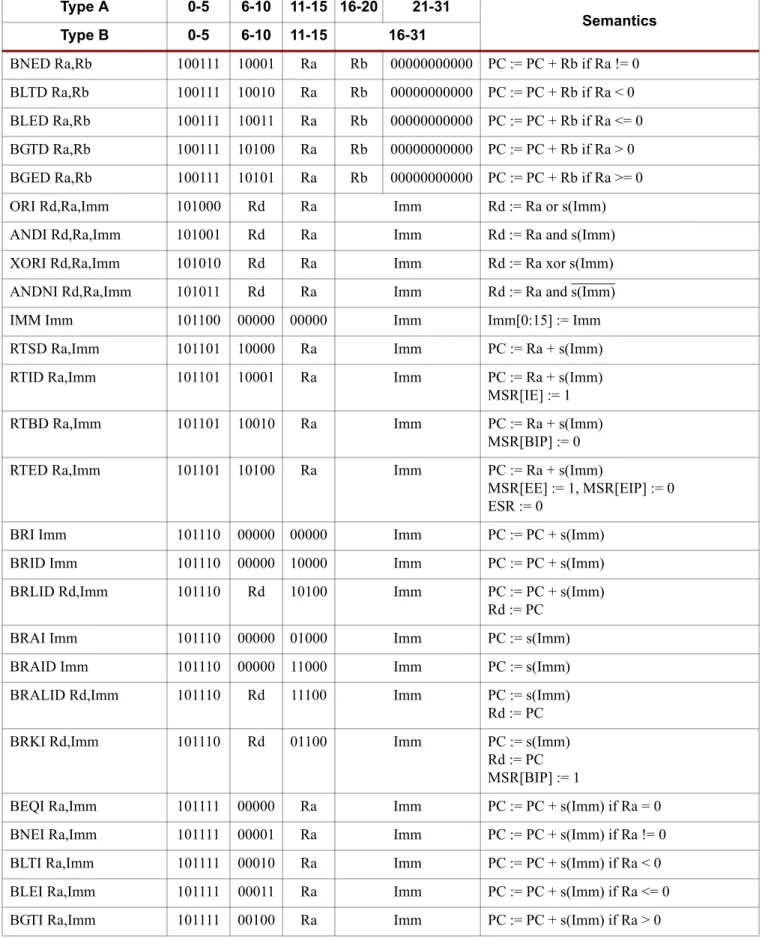
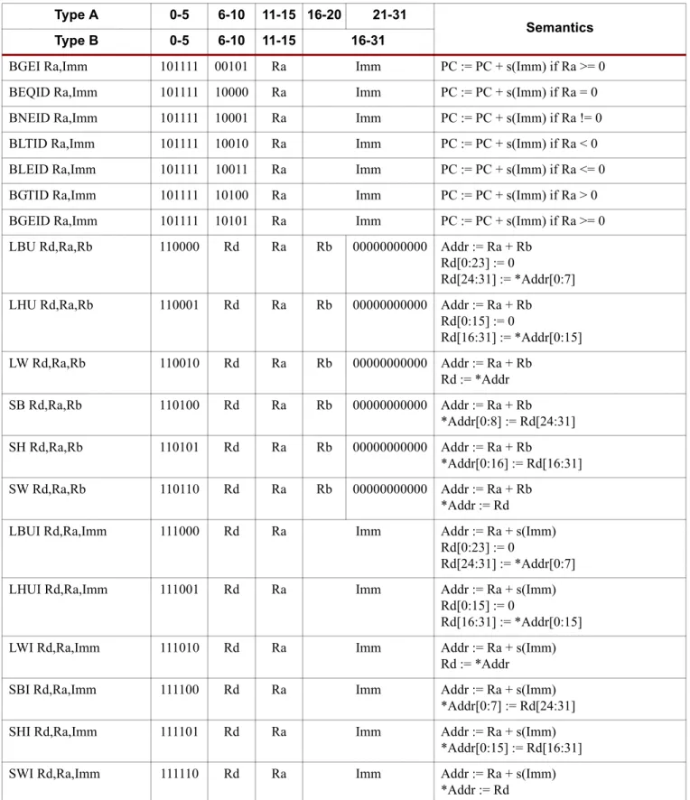
Instructions
All MicroBlaze instructions are 32 bits and are defined as either Type A or Type B. Type A instructions have up to two source register operands and one destination register operand. Type B instructions have one source register and a 16-bit immediate operand (which can be extended to 32 bits by preceding the Type B instruction with an imm instruction). Type B instructions have a single destination register operand. Instructions are provided in the following functional categories:
arithmetic, logical, branch, load/store, and special. Table 1-6 lists the MicroBlaze instruction set.
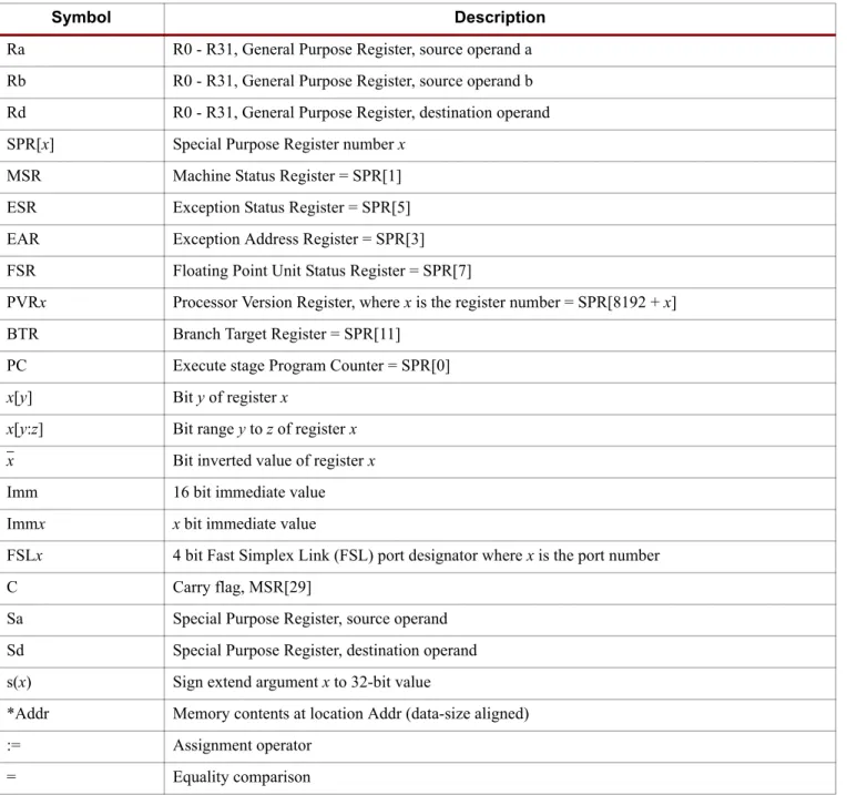
Refer to Chapter 4, “MicroBlaze Instruction Set Architecture”for more information on these instructions. Table 1-5 describes the instruction set nomenclature used in the semantics of each instruction.
Table 1-5: Instruction Set Nomenclature
Symbol Description
Ra R0 - R31, General Purpose Register, source operand a Rb R0 - R31, General Purpose Register, source operand b Rd R0 - R31, General Purpose Register, destination operand SPR[x] Special Purpose Register number x
MSR Machine Status Register = SPR[1]
ESR Exception Status Register = SPR[5]
EAR Exception Address Register = SPR[3]
FSR Floating Point Unit Status Register = SPR[7]
PVRx Processor Version Register, where x is the register number = SPR[8192 + x]
BTR Branch Target Register = SPR[11]
PC Execute stage Program Counter = SPR[0]
x[y] Bit y of register x
x[y:z] Bit range y to z of register x
x Bit inverted value of register x
Imm 16 bit immediate value
Immx x bit immediate value
FSLx 4 bit Fast Simplex Link (FSL) port designator where x is the port number
C Carry flag, MSR[29]
Sa Special Purpose Register, source operand Sd Special Purpose Register, destination operand s(x) Sign extend argument x to 32-bit value
*Addr Memory contents at location Addr (data-size aligned)
:= Assignment operator
!= Inequality comparison
> Greater than comparison
>= Greater than or equal comparison
< Less than comparison
<= Less than or equal comparison
+ Arithmetic add
* Arithmetic multiply
/ Arithmetic divide
>> x Bit shift right x bits
<< x Bit shift left x bits
and Logic AND
or Logic OR
xor Logic exclusive OR
op1 if cond else op2 Perform op1 if condition cond is true, else perform op2
& Concatenate. E.g. “0000100 & Imm7” is the concatenation of the fixed field “0000100” and a 7 bit immediate value.
signed Operation performed on signed integer data type. All arithmetic operations are performed on signed word operands, unless otherwise specified
unsigned Operation performed on unsigned integer data type float Operation performed on floating point data type Table 1-5: Instruction Set Nomenclature (Continued)
Symbol Description
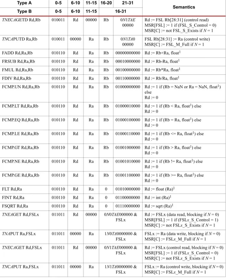
Table 1-6: MicroBlaze Instruction Set Summary
Type A 0-5 6-10 11-15 16-20 21-31
Semantics
Type B 0-5 6-10 11-15 16-31
ADD Rd,Ra,Rb 000000 Rd Ra Rb 00000000000 Rd := Rb + Ra
RSUB Rd,Ra,Rb 000001 Rd Ra Rb 00000000000 Rd := Rb + Ra + 1
ADDC Rd,Ra,Rb 000010 Rd Ra Rb 00000000000 Rd := Rb + Ra + C
RSUBC Rd,Ra,Rb 000011 Rd Ra Rb 00000000000 Rd := Rb + Ra + C
ADDK Rd,Ra,Rb 000100 Rd Ra Rb 00000000000 Rd := Rb + Ra
RSUBK Rd,Ra,Rb 000101 Rd Ra Rb 00000000000 Rd := Rb + Ra + 1
ADDKC Rd,Ra,Rb 000110 Rd Ra Rb 00000000000 Rd := Rb + Ra + C
RSUBKC Rd,Ra,Rb 000111 Rd Ra Rb 00000000000 Rd := Rb + Ra + C
CMP Rd,Ra,Rb 000101 Rd Ra Rb 00000000001 Rd := Rb + Ra + 1
Rd[0] := 0 if (Rb >= Ra) else Rd[0] := 1
CMPU Rd,Ra,Rb 000101 Rd Ra Rb 00000000011 Rd := Rb + Ra + 1 (unsigned)
Rd[0] := 0 if (Rb >= Ra, unsigned) else Rd[0] := 1
ADDI Rd,Ra,Imm 001000 Rd Ra Imm Rd := s(Imm) + Ra
RSUBI Rd,Ra,Imm 001001 Rd Ra Imm Rd := s(Imm) + Ra + 1
ADDIC Rd,Ra,Imm 001010 Rd Ra Imm Rd := s(Imm) + Ra + C
RSUBIC Rd,Ra,Imm 001011 Rd Ra Imm Rd := s(Imm) + Ra + C
ADDIK Rd,Ra,Imm 001100 Rd Ra Imm Rd := s(Imm) + Ra
RSUBIK Rd,Ra,Imm 001101 Rd Ra Imm Rd := s(Imm) + Ra + 1
ADDIKC Rd,Ra,Imm 001110 Rd Ra Imm Rd := s(Imm) + Ra + C
RSUBIKC Rd,Ra,Imm 001111 Rd Ra Imm Rd := s(Imm) + Ra + C
MUL Rd,Ra,Rb 010000 Rd Ra Rb 00000000000 Rd := Ra * Rb
MULH Rd,Ra,Rb 010000 Rd Ra Rb 00000000001 Rd := (Ra * Rb) >> 32 (signed) MULHU Rd,Ra,Rb 010000 Rd Ra Rb 00000000011 Rd := (Ra * Rb) >> 32 (unsigned) MULHSU Rd,Ra,Rb 010000 Rd Ra Rb 00000000010 Rd := (Ra, signed * Rb, unsigned) >> 32
(signed)
BSRA Rd,Ra,Rb 010001 Rd Ra Rb 01000000000 Rd := s(Ra >> Rb) BSLL Rd,Ra,Rb 010001 Rd Ra Rb 10000000000 Rd := (Ra << Rb) & 0
MULI Rd,Ra,Imm 011000 Rd Ra Imm Rd := Ra * s(Imm)
BSRLI Rd,Ra,Imm 011001 Rd Ra 00000000000 &
Imm5
Rd : = 0 & (Ra >> Imm5)
BSRAI Rd,Ra,Imm 011001 Rd Ra 00000010000 &
Imm5
Rd := s(Ra >> Imm5)
BSLLI Rd,Ra,Imm 011001 Rd Ra 00000100000 &
Imm5
Rd := (Ra << Imm5) & 0
IDIV Rd,Ra,Rb 010010 Rd Ra Rb 00000000000 Rd := Rb/Ra
IDIVU Rd,Ra,Rb 010010 Rd Ra Rb 00000000010 Rd := Rb/Ra, unsigned
TNEAGETD Rd,Rb 010011 Rd 00000 Rb 0N0TAE
00000
Rd := FSL Rb[28:31] (data read) MSR[FSL] := 1 if (FSL_S_Control = 1) MSR[C] := not FSL_S_Exists if N = 1 TNAPUTD Ra,Rb 010011 00000 Ra Rb 0N0TA0 FSL Rb[28:31] := Ra (data write) Table 1-6: MicroBlaze Instruction Set Summary (Continued)
Type A 0-5 6-10 11-15 16-20 21-31
Semantics
Type B 0-5 6-10 11-15 16-31
TNECAGETD Rd,Rb 010011 Rd 00000 Rb 0N1TAE 00000
Rd := FSL Rb[28:31] (control read) MSR[FSL] := 1 if (FSL_S_Control = 0) MSR[C] := not FSL_S_Exists if N = 1
TNCAPUTD Ra,Rb 010011 00000 Ra Rb 0N1TA0
00000
FSL Rb[28:31] := Ra (control write) MSR[C] := FSL_M_Full if N = 1
FADD Rd,Ra,Rb 010110 Rd Ra Rb 00000000000 Rd := Rb+Ra, float
1FRSUB Rd,Ra,Rb 010110 Rd Ra Rb 00010000000 Rd := Rb-Ra, float
1FMUL Rd,Ra,Rb 010110 Rd Ra Rb 00100000000 Rd := Rb*Ra, float
1FDIV Rd,Ra,Rb 010110 Rd Ra Rb 00110000000 Rd := Rb/Ra, float
1FCMP.UN Rd,Ra,Rb 010110 Rd Ra Rb 01000000000 Rd := 1 if (Rb = NaN or Ra = NaN, float
1) else
Rd := 0
FCMP.LT Rd,Ra,Rb 010110 Rd Ra Rb 01000010000 Rd := 1 if (Rb < Ra, float
1) else Rd := 0
FCMP.EQ Rd,Ra,Rb 010110 Rd Ra Rb 01000100000 Rd := 1 if (Rb = Ra, float
1) else Rd := 0
FCMP.LE Rd,Ra,Rb 010110 Rd Ra Rb 01000110000 Rd := 1 if (Rb <= Ra, float
1) else Rd := 0
FCMP.GT Rd,Ra,Rb 010110 Rd Ra Rb 01001000000 Rd := 1 if (Rb > Ra, float
1) else Rd := 0
FCMP.NE Rd,Ra,Rb 010110 Rd Ra Rb 01001010000 Rd := 1 if (Rb != Ra, float
1) else Rd := 0
FCMP.GE Rd,Ra,Rb 010110 Rd Ra Rb 01001100000 Rd := 1 if (Rb >= Ra, float
1) else Rd := 0
FLT Rd,Ra 010110 Rd Ra 0 01010000000 Rd := float (Ra)
1FINT Rd,Ra 010110 Rd Ra 0 01100000000 Rd := int (Ra)
1FSQRT Rd,Ra 010110 Rd Ra 0 01110000000 Rd := sqrt (Ra)
1TNEAGET Rd,FSLx 011011 Rd 00000 0N0TAE000000 &
FSLx
Rd := FSLx (data read, blocking if N = 0) MSR[FSL] := 1 if (FSLx_S_Control = 1) MSR[C] := not FSLx_S_Exists if N = 1 TNAPUT Ra,FSLx 011011 00000 Ra 1N0TA0000000 &
FSLx
FSLx := Ra (data write, blocking if N = 0) MSR[C] := FSLx_M_Full if N = 1
TNECAGET Rd,FSLx 011011 Rd 00000 0N1TAE000000 &
FSLx
Rd := FSLx (control read, blocking if N = 0) MSR[FSL] := 1 if (FSLx_S_Control = 0) MSR[C] := not FSLx_S_Exists if N = 1 TNCAPUT Ra,FSLx 011011 00000 Ra 1N1TA0000000 &
FSLx
FSLx := Ra (control write, blocking if N = 0) MSR[C] := FSLx_M_Full if N = 1
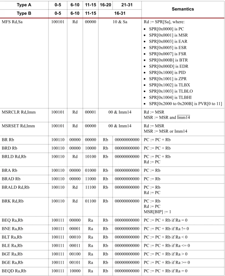
Table 1-6: MicroBlaze Instruction Set Summary (Continued) Type A 0-5 6-10 11-15 16-20 21-31
Semantics
Type B 0-5 6-10 11-15 16-31
OR Rd,Ra,Rb 100000 Rd Ra Rb 00000000000 Rd := Ra or Rb
AND Rd,Ra,Rb 100001 Rd Ra Rb 00000000000 Rd := Ra and Rb
XOR Rd,Ra,Rb 100010 Rd Ra Rb 00000000000 Rd := Ra xor Rb
ANDN Rd,Ra,Rb 100011 Rd Ra Rb 00000000000 Rd := Ra and Rb
PCMPBF Rd,Ra,Rb 100000 Rd Ra Rb 10000000000 Rd := 1 if (Rb[0:7] = Ra[0:7]) else Rd := 2 if (Rb[8:15] = Ra[8:15]) else Rd := 3 if (Rb[16:23] = Ra[16:23]) else Rd := 4 if (Rb[24:31] = Ra[24:31]) else Rd := 0
PCMPEQ Rd,Ra,Rb 100010 Rd Ra Rb 10000000000 Rd := 1 if (Rd = Ra) else Rd := 0
PCMPNE Rd,Ra,Rb 100011 Rd Ra Rb 10000000000 Rd := 1 if (Rd != Ra) else Rd := 0
SRA Rd,Ra 100100 Rd Ra 0000000000000001 Rd := s(Ra >> 1)
C := Ra[31]
SRC Rd,Ra 100100 Rd Ra 0000000000100001 Rd := C & (Ra >> 1) C := Ra[31]
SRL Rd,Ra 100100 Rd Ra 0000000001000001 Rd := 0 & (Ra >> 1) C := Ra[31]
SEXT8 Rd,Ra 100100 Rd Ra 0000000001100000 Rd := s(Ra[24:31])
SEXT16 Rd,Ra 100100 Rd Ra 0000000001100001 Rd := s(Ra[16:31])
WIC Ra,Rb 100100 00000 Ra Rb 01101000 ICache_Line[Ra >> 4].Tag := 0 if (C_ICACHE_LINE_LEN = 4) ICache_Line[Ra >> 5].Tag := 0 if (C_ICACHE_LINE_LEN = 8) WDC Ra,Rb 100100 00000 Ra Rb 01100100 DCache_Line[Ra >> 4].Tag := 0 if
(C_DCACHE_LINE_LEN = 4) DCache_Line[Ra >> 5].Tag := 0 if (C_DCACHE_LINE_LEN = 8)
MTS Sd,Ra 100101 00000 Ra 11 & Sd SPR[Sd] := Ra, where:
• SPR[0x0001] is MSR
• SPR[0x0007] is FSR
• SPR[0x1000] is PID
• SPR[0x1001] is ZPR
• SPR[0x1002] is TLBX
• SPR[0x1003] is TLBLO
• SPR[0x1004] is TLBHI
• SPR[0x1005] is TLBSX Table 1-6: MicroBlaze Instruction Set Summary (Continued)
Type A 0-5 6-10 11-15 16-20 21-31
Semantics
Type B 0-5 6-10 11-15 16-31
MFS Rd,Sa 100101 Rd 00000 10 & Sa Rd := SPR[Sa], where:
• SPR[0x0000] is PC
• SPR[0x0001] is MSR
• SPR[0x0003] is EAR
• SPR[0x0005] is ESR
• SPR[0x0007] is FSR
• SPR[0x000B] is BTR
• SPR[0x000D] is EDR
• SPR[0x1000] is PID
• SPR[0x1001] is ZPR
• SPR[0x1002] is TLBX
• SPR[0x1003] is TLBLO
• SPR[0x1004] is TLBHI
• SPR[0x2000 to 0x200B] is PVR[0 to 11]
MSRCLR Rd,Imm 100101 Rd 00001 00 & Imm14 Rd := MSR
MSR := MSR and Imm14
MSRSET Rd,Imm 100101 Rd 00000 00 & Imm14 Rd := MSR
MSR := MSR or Imm14
BR Rb 100110 00000 00000 Rb 00000000000 PC := PC + Rb
BRD Rb 100110 00000 10000 Rb 00000000000 PC := PC + Rb
BRLD Rd,Rb 100110 Rd 10100 Rb 00000000000 PC := PC + Rb
Rd := PC
BRA Rb 100110 00000 01000 Rb 00000000000 PC := Rb
BRAD Rb 100110 00000 11000 Rb 00000000000 PC := Rb
BRALD Rd,Rb 100110 Rd 11100 Rb 00000000000 PC := Rb
Rd := PC
BRK Rd,Rb 100110 Rd 01100 Rb 00000000000 PC := Rb
Rd := PC MSR[BIP] := 1
BEQ Ra,Rb 100111 00000 Ra Rb 00000000000 PC := PC + Rb if Ra = 0
BNE Ra,Rb 100111 00001 Ra Rb 00000000000 PC := PC + Rb if Ra != 0
BLT Ra,Rb 100111 00010 Ra Rb 00000000000 PC := PC + Rb if Ra < 0
BLE Ra,Rb 100111 00011 Ra Rb 00000000000 PC := PC + Rb if Ra <= 0
BGT Ra,Rb 100111 00100 Ra Rb 00000000000 PC := PC + Rb if Ra > 0
BGE Ra,Rb 100111 00101 Ra Rb 00000000000 PC := PC + Rb if Ra >= 0
BEQD Ra,Rb 100111 10000 Ra Rb 00000000000 PC := PC + Rb if Ra = 0
Table 1-6: MicroBlaze Instruction Set Summary (Continued) Type A 0-5 6-10 11-15 16-20 21-31
Semantics
Type B 0-5 6-10 11-15 16-31
BNED Ra,Rb 100111 10001 Ra Rb 00000000000 PC := PC + Rb if Ra != 0 BLTD Ra,Rb 100111 10010 Ra Rb 00000000000 PC := PC + Rb if Ra < 0 BLED Ra,Rb 100111 10011 Ra Rb 00000000000 PC := PC + Rb if Ra <= 0 BGTD Ra,Rb 100111 10100 Ra Rb 00000000000 PC := PC + Rb if Ra > 0 BGED Ra,Rb 100111 10101 Ra Rb 00000000000 PC := PC + Rb if Ra >= 0
ORI Rd,Ra,Imm 101000 Rd Ra Imm Rd := Ra or s(Imm)
ANDI Rd,Ra,Imm 101001 Rd Ra Imm Rd := Ra and s(Imm)
XORI Rd,Ra,Imm 101010 Rd Ra Imm Rd := Ra xor s(Imm)
ANDNI Rd,Ra,Imm 101011 Rd Ra Imm Rd := Ra and s(Imm)
IMM Imm 101100 00000 00000 Imm Imm[0:15] := Imm
RTSD Ra,Imm 101101 10000 Ra Imm PC := Ra + s(Imm)
RTID Ra,Imm 101101 10001 Ra Imm PC := Ra + s(Imm)
MSR[IE] := 1
RTBD Ra,Imm 101101 10010 Ra Imm PC := Ra + s(Imm)
MSR[BIP] := 0
RTED Ra,Imm 101101 10100 Ra Imm PC := Ra + s(Imm)
MSR[EE] := 1, MSR[EIP] := 0 ESR := 0
BRI Imm 101110 00000 00000 Imm PC := PC + s(Imm)
BRID Imm 101110 00000 10000 Imm PC := PC + s(Imm)
BRLID Rd,Imm 101110 Rd 10100 Imm PC := PC + s(Imm)
Rd := PC
BRAI Imm 101110 00000 01000 Imm PC := s(Imm)
BRAID Imm 101110 00000 11000 Imm PC := s(Imm)
BRALID Rd,Imm 101110 Rd 11100 Imm PC := s(Imm)
Rd := PC
BRKI Rd,Imm 101110 Rd 01100 Imm PC := s(Imm)
Rd := PC MSR[BIP] := 1
BEQI Ra,Imm 101111 00000 Ra Imm PC := PC + s(Imm) if Ra = 0
BNEI Ra,Imm 101111 00001 Ra Imm PC := PC + s(Imm) if Ra != 0
BLTI Ra,Imm 101111 00010 Ra Imm PC := PC + s(Imm) if Ra < 0
BLEI Ra,Imm 101111 00011 Ra Imm PC := PC + s(Imm) if Ra <= 0
Table 1-6: MicroBlaze Instruction Set Summary (Continued) Type A 0-5 6-10 11-15 16-20 21-31
Semantics
Type B 0-5 6-10 11-15 16-31
BGEI Ra,Imm 101111 00101 Ra Imm PC := PC + s(Imm) if Ra >= 0
BEQID Ra,Imm 101111 10000 Ra Imm PC := PC + s(Imm) if Ra = 0
BNEID Ra,Imm 101111 10001 Ra Imm PC := PC + s(Imm) if Ra != 0
BLTID Ra,Imm 101111 10010 Ra Imm PC := PC + s(Imm) if Ra < 0
BLEID Ra,Imm 101111 10011 Ra Imm PC := PC + s(Imm) if Ra <= 0
BGTID Ra,Imm 101111 10100 Ra Imm PC := PC + s(Imm) if Ra > 0
BGEID Ra,Imm 101111 10101 Ra Imm PC := PC + s(Imm) if Ra >= 0
LBU Rd,Ra,Rb 110000 Rd Ra Rb 00000000000 Addr := Ra + Rb
Rd[0:23] := 0
Rd[24:31] := *Addr[0:7]
LHU Rd,Ra,Rb 110001 Rd Ra Rb 00000000000 Addr := Ra + Rb
Rd[0:15] := 0
Rd[16:31] := *Addr[0:15]
LW Rd,Ra,Rb 110010 Rd Ra Rb 00000000000 Addr := Ra + Rb
Rd := *Addr
SB Rd,Ra,Rb 110100 Rd Ra Rb 00000000000 Addr := Ra + Rb
*Addr[0:8] := Rd[24:31]
SH Rd,Ra,Rb 110101 Rd Ra Rb 00000000000 Addr := Ra + Rb
*Addr[0:16] := Rd[16:31]
SW Rd,Ra,Rb 110110 Rd Ra Rb 00000000000 Addr := Ra + Rb
*Addr := Rd
LBUI Rd,Ra,Imm 111000 Rd Ra Imm Addr := Ra + s(Imm)
Rd[0:23] := 0
Rd[24:31] := *Addr[0:7]
LHUI Rd,Ra,Imm 111001 Rd Ra Imm Addr := Ra + s(Imm)
Rd[0:15] := 0
Rd[16:31] := *Addr[0:15]
LWI Rd,Ra,Imm 111010 Rd Ra Imm Addr := Ra + s(Imm)
Rd := *Addr
SBI Rd,Ra,Imm 111100 Rd Ra Imm Addr := Ra + s(Imm)
*Addr[0:7] := Rd[24:31]
SHI Rd,Ra,Imm 111101 Rd Ra Imm Addr := Ra + s(Imm)
*Addr[0:15] := Rd[16:31]
SWI Rd,Ra,Imm 111110 Rd Ra Imm Addr := Ra + s(Imm)
*Addr := Rd
1. Due to the many different corner cases involved in floating point arithmetic, only the normal behavior is described. A full description of the behavior can be found in Chapter 4, “MicroBlaze Instruction Set Architecture.”
Table 1-6: MicroBlaze Instruction Set Summary (Continued) Type A 0-5 6-10 11-15 16-20 21-31
Semantics
Type B 0-5 6-10 11-15 16-31
Registers
MicroBlaze has an orthogonal instruction set architecture. It has thirty-two 32-bit general purpose registers and up to eighteen 32-bit special purpose registers, depending on configured options.
General Purpose Registers
The thirty-two 32-bit General Purpose Registers are numbered R0 through R31. The register file is reset on bit stream download (reset value is 0x00000000). Figure 1-2 is a representation of a General Purpose Register and Table 1-7 provides a description of each register and the register reset value (if existing).
Note: The register file is not reset by the external reset inputs: Reset and Debug_Rst.
Refer to Table 3-2 for software conventions on general purpose register usage.
0 31
↑ R0-R31
Figure 1-2: R0-R31
Table 1-7: General Purpose Registers (R0-R31)
Bits Name Description Reset Value
0:31 R0 Always has a value of zero. Anything written to
R0 is discarded 0x00000000
0:31 R1 through R13 32-bit general purpose registers -
0:31 R14 32-bit register used to store return addresses for interrupts.
- 0:31 R15 32-bit general purpose register. Recommended
for storing return addresses for user vectors.
- 0:31 R16 32-bit register used to store return addresses
for breaks.
- 0:31 R17 If MicroBlaze is configured to support
hardware exceptions, this register is loaded with the address of the instruction following the instruction causing the HW exception, except for exceptions in delay slots that use BTR instead (see “Branch Target Register (BTR)”); if not, it is a general purpose register.
-
0:31 R18 through R31 R18 through R31 are 32-bit general purpose registers.
-
Special Purpose Registers
Program Counter (PC)
The Program Counter (PC) is the 32-bit address of the execution instruction. It can be read with an MFS instruction, but it cannot be written with an MTS instruction. When used with the MFS instruction the PC register is specified by setting Sa = 0x0000. Figure 1-3 illustrates the PC and Table 1-8 provides a description and reset value.
Machine Status Register (MSR)
The Machine Status Register contains control and status bits for the processor. It can be read with an MFS instruction. When reading the MSR, bit 29 is replicated in bit 0 as the carry copy. MSR can be written using either an MTS instruction or the dedicated MSRSET and MSRCLR instructions.
When writing to the MSR, the Carry bit takes effect immediately and the remaining bits take effect one clock cycle later. Any value written to bit 0 is discarded. When used with an MTS or MFS instruction, the MSR is specified by setting Sx = 0x0001. Figure 1-4 illustrates the MSR register and Table 1-9 provides the bit description and reset values.
0 31
↑ PC
Figure 1-3: PC
Table 1-8: Program Counter (PC)
Bits Name Description Reset Value
0:31 PC Program Counter
Address of executing instruction, that is, “mfs r2 0” stores the address of the mfs instruction itself in R2.
0x00000000
0 17 18 19 20 21 22 23 24 25 26 27 28 29 30 31
↑ ↑ ↑ ↑ ↑ ↑ ↑ ↑ ↑ ↑ ↑ ↑ ↑ ↑ ↑ ↑ ↑
CC RESERVED VMS VM UMS UMPVR EIP EE DCE DZ ICE FSL BIP C IE BE
Figure 1-4: MSR
Table 1-9: Machine Status Register (MSR)
Bits Name Description Reset Value
0 CC Arithmetic Carry Copy
Copy of the Arithmetic Carry (bit 29). CC is always the same as bit C.
0
1:16 Reserved
17 VMS Virtual Protected Mode Save
Only available when configured with an MMU (if C_USE_MMU>1)
Read/Write
0
18 VM Virtual Protected Mode
0 MMU address translation and access protection disabled, with C_USE_MMU = 3.
Access protection disabled, with C_USE_MMU
= 2.
1 MMU address translation and access protection enabled, with C_USE_MMU = 3.
Access protection enabled, with C_USE_MMU
= 2.
Only available when configured with an MMU (if C_USE_MMU>1)
Read/Write
0
19 UMS User Mode Save
Only available when configured with an MMU (if C_USE_MMU>0)
Read/Write
0
20 UM User Mode
0 Privileged Mode, all instructions are allowed 1 User Mode, certain instructions are not allowed
Only available when configured with an MMU (if C_USE_MMU>0)
Read/Write
0
21 PVR Processor Version Register exists 0 No Processor Version Register 1 Processor Version Register exists Read only
Based on
parameter
C_PVR
22 EIP Exception In Progress
0 = No hardware exception in progress 1 = Hardware exception in progress
Only available if configured with exception support (C_*_EXCEPTION or C_USE_MMU) Read/Write
0
23 EE Exception Enable
0 = Hardware exceptions disabled
11 = Hardware exceptions enabled
Only available if configured with exception support (C_*_EXCEPTION or C_USE_MMU) Read/Write
0
24 DCE Data Cache Enable
0 = Data Cache disabled 1 = Data Cache enabled
Only available if configured to use data cache (C_USE_DCACHE = 1)
Read/Write
0
25 DZ Division by Zero
20 = No division by zero has occurred 1 = Division by zero has occurred
Only available if configured to use hardware divider (C_USE_DIV = 1)
Read/Write
0
26 ICE Instruction Cache Enable 0 = Instruction Cache disabled 1 = Instruction Cache enabled
Only available if configured to use instruction cache (C_USE_ICACHE = 1)
Read/Write
0
27 FSL FSL Error
0 = FSL get/getd/put/putd had no error
1 = FSL get/getd/put/putd control type mismatch Only available if configured to use FSL links (C_FSL_LINKS > 0)
Read/Write
0 Table 1-9: Machine Status Register (MSR) (Continued)
Bits Name Description Reset Value
28 BIP Break in Progress 0 = No Break in Progress 1 = Break in Progress
Break Sources can be software break instruction or hardware break from Ext_Brk or
Ext_NM_Brk pin.
Read/Write
0
29 C Arithmetic Carry
0 = No Carry (Borrow) 1 = Carry (No Borrow) Read/Write
0
30 IE Interrupt Enable
0 = Interrupts disabled 1 = Interrupts enabled Read/Write
0
31 BE Buslock Enable
30 = Buslock disabled on data-side OPB 1 = Buslock enabled on data-side OPB Buslock Enable does not affect operation of IXCL, DXCL, ILMB, DLMB, IPLB, DPLB or IOPB.
Only available if using data-side OPB Read/Write
0
1. The MMU exceptions (Data Storage Exception, Instruction Storage Exception, Data TLB Miss Exception, Instruction TLB Miss Exception) cannot be disabled, and are not affected by this bit.
2. This bit is only used for integer divide-by-zero signaling. There is a floating point equivalent in the FSR.
The DZ-bit flags divide by zero conditions regardless if the processor is configured with exception handling or not.
3. For details on the bus protocols, refer to the IBM CoreConnect specification:
64-Bit On-Chip Peripheral Bus, Architectural Specifications, Version 2.0
.Table 1-9: Machine Status Register (MSR) (Continued)
Bits Name Description Reset Value
Exception Address Register (EAR)
The Exception Address Register stores the full load/store address that caused the exception for the following:
• An unaligned access exception that means the unaligned access address
• A DPLB or DOPB exception that specifies the failing PLB or OPB data access address
• A data storage exception that specifies the (virtual) effective address accessed
• An instruction storage exception that specifies the (virtual) effective address read
• A data TLB miss exception that specifies the (virtual) effective address accessed
• An instruction TLB miss exception that specifies the (virtual) effective address read The contents of this register is undefined for all other exceptions. When read with the MFS instruction, the EAR is specified by setting Sa = 0x0003. The EAR register is illustrated in Figure 1-5 and Table 1-10 provides bit descriptions and reset values.
0 31
↑ EAR
Figure 1-5: EAR
Table 1-10: Exception Address Register (EAR)
Bits Name Description Reset Value
0:31 EAR Exception Address Register 0x00000000
Exception Status Register (ESR)
The Exception Status Register contains status bits for the processor. When read with the MFS instruction, the ESR is specified by setting Sa = 0x0005. The ESR register is illustrated in Figure 1-6, Table 1-11 provides bit descriptions and reset values, and Table 1-12 provides the Exception Specific Status (ESS).
19 20 26 27 31
↑ ↑ ¦ ↑
RESERVED DS ESS EC
Figure 1-6: ESR
Table 1-11: Exception Status Register (ESR)
Bits Name Description Reset Value
0:18 Reserved
19 DS Delay Slot Exception.
0 = not caused by delay slot instruction 1 = caused by delay slot instruction Read-only
0
20:26 ESS Exception Specific Status For details refer to Table 1-12.
Read-only
See Table 1-12
27:31 EC Exception Cause
00000 = Fast Simplex Link exception 00001 = Unaligned data access exception 00010 = Illegal op-code exception 00011 = Instruction bus error exception 00100 = Data bus error exception 00101 = Divide by zero exception 00110 = Floating point unit exception 00111 = Privileged instruction exception 10000 = Data storage exception
10001 = Instruction storage exception 10010 = Data TLB miss exception 10011 = Instruction TLB miss exception Read-only
0
Table 1-12: Exception Specific Status (ESS) Exception
Cause Bits Name Description Reset Value
Unaligned Data Access
20 W Word Access Exception
0 = unaligned halfword access 1 = unaligned word access
0
21 S Store Access Exception
0 = unaligned load access 1 = unaligned store access
0
22:26 Rx Source/Destination Register
General purpose register used as source (Store) or destination (Load) in unaligned access
0
Illegal Instruction
20:26 Reserved 0
Instruction bus error
20:26 Reserved 0
Data bus error
20:26 Reserved 0
Divide by zero
20:26 Reserved 0
Floating point unit
20:26 Reserved 0
Privileged instruction
20:26 Reserved 0
Fast Simplex Link
20:22 Reserved 0
23:26 FSL Fast Simplex Link index that caused the exception
0 Data storage 20 DIZ Data storage - Zone protection
0 = Did not occur 1 = Occurred
0
21 S Data storage - Store instruction
0 = Did not occur 1 = Occurred
0
22:26 Reserved 0
Instruction storage
20 DIZ Instruction storage - Zone protection 0 = Did not occur
1 = Occurred
0
21:26 Reserved 0
Branch Target Register (BTR)
The Branch Target Register only exists if the MicroBlaze processor is configured to use exceptions.
The register stores the branch target address for all delay slot branch instructions executed while MSR[EIP] = 0. If an exception is caused by an instruction in a delay slot (that is, ESR[DS]=1), the exception handler should return execution to the address stored in BTR instead of the normal exception return address stored in R17. When read with the MFS instruction, the BTR is specified by setting Sa = 0x000B. The BTR register is illustrated in Figure 1-7 and Table 1-13 provides bit descriptions and reset values.
Data TLB miss
20 Reserved 0
21 S Data TLB miss - Store instruction
0 = Did not occur 1 = Occurred
0
22:26 Reserved 0
Instruction TLB miss
20:26 Reserved 0
Table 1-12: Exception Specific Status (ESS) (Continued) Exception
Cause Bits Name Description Reset Value
0 31
↑ BTR
Figure 1-7: BTR
Table 1-13: Branch Target Register (BTR)
Bits Name Description Reset Value
0:31 BTR Branch target address used by handler when returning from an exception caused by an instruction in a delay slot.
Read-only
0x00000000
Floating Point Status Register (FSR)
The Floating Point Status Register contains status bits for the floating point unit. It can be read with an MFS, and written with an MTS instruction. When read or written, the register is specified by setting Sa = 0x0007. Figure 1-8 illustrates the FSR register and Table 1-14 provides bit descriptions and reset values.
27 28 29 30 31
↑ ↑ ↑ ↑ ↑ ↑
RESERVED IO DZ OF UF DO
Exception Data Register (EDR)
The Exception Data Register stores data read on an FSL link that caused an FSL exception.
The contents of this register is undefined for all other exceptions. When read with the MFS instruction, the EDR is specified by setting Sa = 0x000D. Figure 1-9 illustrates the EDR register and Table 1-15 provides bit descriptions and reset values.
Note: The register is only implemented if C_FSL_LINKS is greater than 0 and C_FSL_EXCEPTION is set to 1.
Figure 1-8: FSR
Table 1-14: Floating Point Status Register (FSR)
Bits Name Description Reset Value
0:26 Reserved undefined
27 IO Invalid operation 0
28 DZ Divide-by-zero 0
29 OF Overflow 0
30 UF Underflow 0
31 DO Denormalized operand error 0
0 31
↑ EDR
Figure 1-9: EDR
Table 1-15: Exception Data Register (EDR)
Bits Name Description Reset Value
0:31 EDR Exception Data Register 0x00000000
Process Identifier Register (PID)
The Process Identifier Register is used to uniquely identify a software process during MMU address translation. It is controlled by the C_MMU configuration option on MicroBlaze. The register is only implemented if C_MMU is greater than 1. When accessed with the MFS and MTS instructions, the PID is specified by setting Sa = 0x1000. The register is accessible according to the memory management special registers parameter C_MMU_TLB_ACCESS.
PID is also used when accessing a TLB entry:
• When writing Translation Look-Aside Buffer High (TLBHI) the value of PID is stored in the TID field of the TLB entry
• When reading TLBHI the value in the TID field is stored in PID
Figure 1-10 illustrates the PID register and Table 1-16 provides bit descriptions and reset values.
24 31
↑ ↑
RESERVED PID
Figure 1-10: PID
Table 1-16: Process Identifier Register (PID)
Bits Name Description Reset Value
0:23 Reserved
24:31 PID Used to uniquely identify a software process during MMU address translation.
Read/Write
0x00
Zone Protection Register (ZPR)
The Zone Protection Register is used to override MMU memory protection defined in TLB entries.
It is controlled by the C_MMU configuration option on MicroBlaze. The register is only implemented if C_MMU is greater than 1 and if the number of specified memory protection zones is greater than zero (C_MMU_ZONES > 0). The implemented register bits depend on the number of specified memory protection zones (C_MMU_ZONES). When accessed with the MFS and MTS instructions, the ZPR is specified by setting Sa = 0x1001. The register is accessible according to the memory management special registers parameter C_MMU_TLB_ACCESS. Figure 1-11 illustrates the ZPR register and Table 1-17 provides bit descriptions and reset values.
0 2 4 6 8 10 12 14 16 18 20 22 24 26 28 30
↑ ↑ ↑ ↑ ↑ ↑ ↑ ↑ ↑ ↑ ↑ ↑ ↑ ↑ ↑ ↑
ZP0 ZP1 ZP2 ZP3 ZP4 ZP5 ZP6 ZP7 ZP8 ZP9 ZP10 ZP11 ZP12 ZP13 ZP14 ZP15
Figure 1-11: ZPR
Table 1-17: Zone Protection Register (ZPR)
Bits Name Description Reset Value
0:1 2:3 ...
30:31 ZP0 ZP1 ...
ZP15
Zone Protect
User mode (MSR[UM] = 1):
00 = Override V in TLB entry. No access to the page is allowed
01 = No override. Use V, WR and EX from TLB entry 10 = No override. Use V, WR and EX from TLB entry 11 = Override WR and EX in TLB entry. Access the page as writable and executable
Privileged mode (MSR[UM] = 0):
00 = No override. Use V, WR and EX from TLB entry 01 = No override. Use V, WR and EX from TLB entry 10 = Override WR and EX in TLB entry. Access the page as writable and executable
11 = Override WR and EX in TLB entry. Access the page as writable and executable
Read/Write
0x00000000
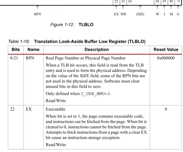
Translation Look-Aside Buffer Low Register (TLBLO)
The Translation Look-Aside Buffer Low Register is used to access MMU Unified Translation Look- Aside Buffer (UTLB) entries. It is controlled by the C_MMU configuration option on MicroBlaze.
The register is only implemented if C_MMU is greater than 1. When accessed with the MFS and MTS instructions, the TLBLO is specified by setting Sa = 0x1003. When reading or writing TLBLO, the UTLB entry indexed by the TLBX register is accessed. The register is readable according to the memory management special registers parameter C_MMU_TLB_ACCESS.
The UTLB is reset on bit stream download (reset value is 0x00000000 for all TLBLO entries).
Note: The UTLB is not reset by the external reset inputs: Reset and Debug_Rst.
Figure 1-12 illustrates the TLBLO register and Table 1-18 provides bit descriptions and reset values.
0 22 23 24 28 29 30 31
↑ ↑ ↑ ↑ ↑ ↑ ↑ ↑
RPN EX WR ZSEL W I M G
Figure 1-12: TLBLO
Table 1-18: Translation Look-Aside Buffer Low Register (TLBLO)
Bits Name Description Reset Value
0:21 RPN Real Page Number or Physical Page Number
When a TLB hit occurs, this field is read from the TLB entry and is used to form the physical address. Depending on the value of the SIZE field, some of the RPN bits are not used in the physical address. Software must clear unused bits in this field to zero.
Only defined when C_USE_MMU=3.
Read/Write
0x000000
22 EX Executable
When bit is set to 1, the page contains executable code, and instructions can be fetched from the page. When bit is cleared to 0, instructions cannot be fetched from the page.
Attempts to fetch instructions from a page with a clear EX bit cause an instruction-storage exception.
Read/Write
0
23 WR Writable
When bit is set to 1, the page is writable and store instructions can be used to store data at addresses within the page.
When bit is cleared to 0, the page is read-only (not writable). Attempts to store data into a page with a clear WR bit cause a data storage exception.
Read/Write
0
24:27 ZSEL Zone Select
This field selects one of 16 zone fields (Z0-Z15) from the zone-protection register (ZPR).
For example, if ZSEL 0x5, zone field Z5 is selected. The selected ZPR field is used to modify the access protection specified by the TLB entry EX and WR fields. It is also used to prevent access to a page by overriding the TLB V (valid) field.
Read/Write
0x0
28 W Write Through
This bit is fixed to 1, because accesses to pages on MicroBlaze are always cached using a write-through caching policy.
Read Only
1
29 I Inhibit Caching
When bit is set to 1, accesses to the page are not cached (caching is inhibited).
When cleared to 0, accesses to the page are cacheable.
Read/Write
0
30 M Memory Coherent
This bit is fixed to 0, because memory coherence is not implemented on MicroBlaze.
Read Only
0
31 G Guarded
When bit is set to 1, speculative page accesses are not allowed (memory is guarded).
When cleared to 0, speculative page accesses are allowed.
The G attribute can be used to protect memory-mapped I/O devices from inappropriate instruction accesses.
Read/Write
0 Table 1-18: Translation Look-Aside Buffer Low Register (TLBLO) (Continued)
Bits Name Description Reset Value
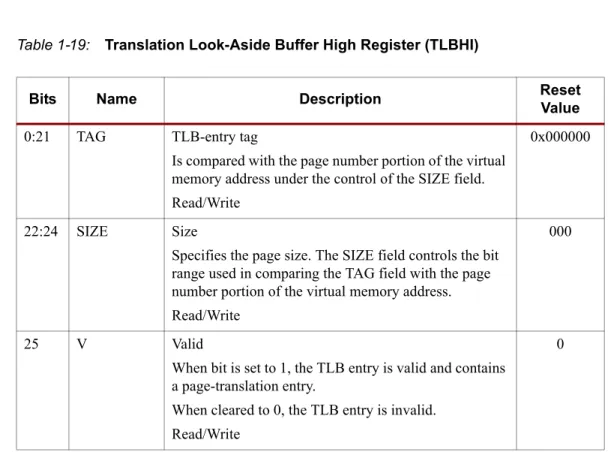
Translation Look-Aside Buffer High Register (TLBHI)
The Translation Look-Aside Buffer High Register is used to access MMU Unified Translation Look-Aside Buffer (UTLB) entries. It is controlled by the C_MMU configuration option on MicroBlaze. The register is only implemented if C_MMU is greater than 1. When accessed with the MFS and MTS instructions, the TLBHI is specified by setting Sa = 0x1004. When reading or writing TLBHI, the UTLB entry indexed by the TLBX register is accessed. The register is readable according to the memory management special registers parameter C_MMU_TLB_ACCESS.
PID is also used when accessing a TLB entry:
• When writing TLBHI the value of PID is stored in the TID field of the TLB entry
• When reading TLBHI the value in the TID field is stored in PID
The UTLB is reset on bit stream download (reset value is 0x00000000 for all TLBHI entries).
Note: The UTLB is not reset by the external reset inputs: Reset and Debug_Rst.
Figure 1-13 illustrates the TLBHI register and Table 1-19 provides bit descriptions and reset values.
0 22 25 26 27 28 31
↑ ↑ ↑ ↑ ↑ ↑
TAG SIZE V E U0 Reserved
Figure 1-13: TLBHI
Table 1-19: Translation Look-Aside Buffer High Register (TLBHI)
Bits Name Description Reset
Value
0:21 TAG TLB-entry tag
Is compared with the page number portion of the virtual memory address under the control of the SIZE field.
Read/Write
0x000000
22:24 SIZE Size
Specifies the page size. The SIZE field controls the bit range used in comparing the TAG field with the page number portion of the virtual memory address.
Read/Write
000
25 V Valid
When bit is set to 1, the TLB entry is valid and contains a page-translation entry.
When cleared to 0, the TLB entry is invalid.
Read/Write
0
26 E Endian
This bit is fixed to 0, since accesses to pages on MicroBlaze are always big endian.
Read Only
0
27 U0 User Defined
This bit is fixed to 0, since there are no user defined storage attributes on MicroBlaze.
Read Only
0
28:31 Reserved
Table 1-19: Translation Look-Aside Buffer High Register (TLBHI) (Continued) (Continued)
Bits Name Description Reset
Value
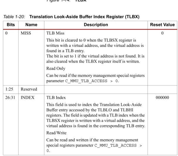
Translation Look-Aside Buffer Index Register (TLBX)
The Translation Look-Aside Buffer Index Register is used as an index to the Unified Translation Look-Aside Buffer (UTLB) when accessing the TLBLO and TLBHI registers. It is controlled by the C_MMU configuration option on MicroBlaze. The register is only implemented if C_MMU is greater than 1. When accessed with the MFS and MTS instructions, the TLBX is specified by setting Sa = 0x1002. Figure 1-14 illustrates the TLBX register and Table 1-20 provides bit descriptions and reset values.
0 26 31
↑ ↑ ↑
MISS Reserved INDEX
Figure 1-14: TLBX
Table 1-20: Translation Look-Aside Buffer Index Register (TLBX)
Bits Name Description Reset Value
0 MISS TLB Miss
This bit is cleared to 0 when the TLBSX register is written with a virtual address, and the virtual address is found in a TLB entry.
The bit is set to 1 if the virtual address is not found. It is also cleared when the TLBX register itself is written.
Read Only
Can be read if the memory management special registers parameter C_MMU_TLB_ACCESS > 0.
0
1:25 Reserved
26:31 INDEX TLB Index
This field is used to index the Translation Look-Aside Buffer entry accessed by the TLBLO and TLBHI registers. The field is updated with a TLB index when the TLBSX register is written with a virtual address, and the virtual address is found in the corresponding TLB entry.
Read/Write
Can be read and written if the memory management special registers parameter C_MMU_TLB_ACCESS >
0.
000000
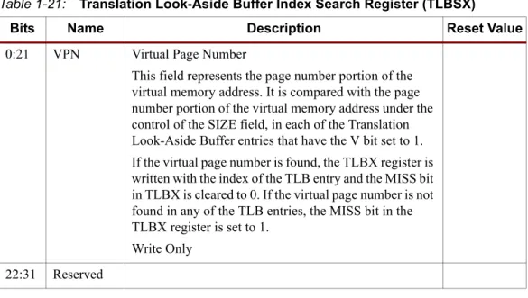
Translation Look-Aside Buffer Search Index Register (TLBSX)
The Translation Look-Aside Buffer Search Index Register is used to search for a virtual page number in the Unified Translation Look-Aside Buffer (UTLB). It is controlled by the C_MMU configuration option on MicroBlaze. The register is only implemented if C_MMU is greater than 1.
When written with the MTS instruction, the TLBSX is specified by setting Sa = 0x1005.
Figure 1-15 illustrates the TLBSX register and Table 1-21 provides bit descriptions and reset values.
0 22 31
↑ ↑
VPN Reserved